Friday, December 27, 2013

Amplifier simple easy and cheap with IC TA7368P

Indeed , this amplifier is suitable known as the title above. Viewed from the schematic alreaady seen that this amplifier circuit requires little components and parts were cheap. This amplifier requires 1 piece of IC TA7368P is manufactered by TOSHIBA is the price too low, then in addition to IC amplifier requires 3 components elco capacitor whose value is not too big. Maybe if you make this amplifier circuit, the total price of all must not be more than $ 1. This amplifier only has more than 1W output, perhaps because it has little strengthening it so that the output is released is very small. But to make this is quite easy and not too costly.
cheap amplifier
Part List :

Capacitor
C1 = 100 uF
C2 = 100uF
C3 = 470uF

IC
IC1 = TA7368P


Good Luck :)
Read More..

LED Phototherapy Unit

It
is widely thought that light can be therapeutic for the human skin and
soul. Light at the correct wavelength may also be effective against
depression and allergies. There is a wide range of products on the
market, at prices from a few tens of pounds to a hundred pounds or so,
which are presented as universal remedies for dust allergies or hay
fever. If we look at these devices in more detail, we find that their
operation is relatively simple to explain.

Common to all the
devices is that they emit intense red light with a wavelength of 660 nm.
Some biophysicists claim that light of this wavelength can have a
positive effect on the human body and can initiate healing processes.
This so-called ‘phototherapy’ is a treatment which is claimed to have an
effect against allergic reactions in the body, since it acts against
free oxygen radicals and strengthens the immune system, reducing
inflammation of the mucous membrane.

Since this treatment does
not take the form of a medicine, but rather the form of visible light,
there is no risk of side-effects. There has been scientific research
showing that this therapy does not work in every case, but success rates
as high as 72 % have been reported. Since it may not be possible to
obtain these devices under the NHS or under private medical insurance,
our thoughts naturally turn to do-it-yourself. For the enclosure we
decided to use an old nasal hair trimmer.


LED Phototherapy Unit circuit schematic

These
can be obtained new for a few pounds, or you may have an old one that
can be recycled. The choice of enclosure also dictates the choice of
battery: the unit contains a holder for an AA-size cell. The circuit
must therefore not only be very compact (there is little spare room in
the enclosure), it must also be able to drive a high-brightness red LED
from a voltage between 1 V and around 1.6 V. Here again we can indulge
in a little recycling: we can re-use the circuit from a Mini Project by
Burkhard Kainka for driving a white LED, published in Elektor
Electronics in June 2002.

In this circuit the inductive voltage
pulse is limited by the LED itself, ensuring that the output voltage
will automatically match the forward voltage of the LED. The circuit is
suitable as it stands for driving a high-brightness 660 nm red LED to
make a do-it-yourself phototherapy unit. In view of the small number of
components, the circuit can be assembled by soldering them together
directly or by using a small piece of stripboard.

The circuit can
operate from a wide range of voltages, and so we can use either an
alkaline AA cell or an AA-size NiMH rechargeable cell with a voltage of
1.2 V. The current consumption of the circuit is about 20 mA. Assuming
the circuit has been built correctly, the red LED should light brightly
as soon as power is applied. Five to ten minutes’ use in each nostril
every day should be sufficient to obtain noticeable benefit after two
weeks of treatment.
Read More..

Thursday, December 26, 2013

High pass and low pass filters

Subsonic and ultrasonic filters can be combined into a single circuit for more stable and orderly bandwith. This good and qualified for only two frequencies with the rotation of widely separate. Circuit schematic above shows the rotation of the scond-order or high-pass Butterworth filter in combination with secon-order low-pass filter.
op amp bass
Part List :
R1___1K
R2___1K
R3___12K
R4___24K
C1___4n4
C2___2n2
C3___470nF
C4___470nF
IC___IC op-amp

For the capacitor , use the ceramic capacitors .
Read More..

Battery Charger with Temeperature Sensor

Battery Charger with Temeperature Sensor


Battery with a LM35 temperature sensor on the charger used to monitor the battery temperature is in charge. Battery temperature sensor is needed because the battery temperature will rise at the time in charge. Battery temperature sensor LM35 temperature sensor has high accuracy in monitoring the battery temperature, it is because the temperature sensor LM35 is a temperature sensor that can convert temperature changes into voltage changes linearly.


At the time of the charge a battery will experience changes in temperature, where the battery temperature will begin to rise when the battery began to fill. To avoid over heat the battery, the battery temperature sensor LM35 temperature sensor is required to terminate the battery charging current to avoid overheating.

battery charger schematic with LM35
Battery charger with temperature sensor schematic

On the battery charger circuit temperature sensor with temperature sensor 35 lm above the R1 is used for setting the maximum value of the desired temperature. Therefore, when the temperature was in-charge the battery begins to rise and reach temperatures setup then this series will break the current battery charge.
Read More..

Mini Stereo Power Amplifier using TDA2822

This circuit TDA2822 total to the same extent your primary device. The Dual Amplifier IC before IC stereo increase by 40 dB. Bandwidth 120 kHZ. with the purpose of is regarding 2 watts and watt power supply of 1.8 to 15 volts and a current 6 mA no more than after using the power supply 9 volt into this circuit.VR1 and VR2 to adjust the suggest level of the best and not here, the pin 7 and pin 6 of IC1.The amplifier IC1 is outmoded of the output pin 1 and pin 3, through the C4 and C5 coupling signals to the absent and right speakers.The C6, R1 and C7, R2 is to reduce blast.

Mini Stereo Power Amplifier using TDA2822 Circuit Diagram

Read More..

Wednesday, December 25, 2013

1 6 Watt intregated circuit audio amplifier

This Circut based on IC TDA7231 , Minimum voltage require 2 Volts and maximum voltage 15 volts . I recomended voltage is 12 volt DC. Power output 1,6 Watt with 4 Ohm impedance. See audio amplifier with IC TDA7231 below :
Read More..

Error Correction Output Stage for Mosfet and BJT Power Amplifier

For best results, any active device with the exception of the output transistors operating in class A. This is to avoid bias to saturate or block the entrance to all the clipping level, should be selected. This raises some difficulties for a BJT amplifier, where (to stay in Class A) driver stage collector currents, the base of BJT output current at maximum output current (ie in our case some of 10A) No is not exceeded. Therefore, the overall bias regime redesigned to allow space for the swing base BJT output current.

Error Correction Output Stage for Mosfet and BJT Power Amplifier

Even in these circumstances, the power dissipation in the driver’s relevant and it is doubtful if a heat sink on board (as in our design side MOSFET included) help, if maximum performance is desired 200W into 4 ohms. It is therefore assumed that the power BJT design based on our application can not be more than one goal and 100W/4ohm 50W/8ohm. Of course, for such relatively modest achievements, it is not necessary to install three pairs of output devices, a pair of (ex) MJL4281/MJL4302 or equivalent work will be done.

Adjusting the balance Hawks Word is a double potentiometer (minimum of ten rounds) with more than 0.5% of correspondence between the sections. We replaced R20 and R81 with a 2K potentiometer Bourns 10 turns and adjusted for minimum distortion 20kHz Open Loop. You will find that the minimum is strongly dependent on the frequency, always adapting to at least the higher frequency in the audible range. At low frequencies, the feedback loop gain in reducing DHT levels to help you. Measured values ??and replace the potentiometer with fixed resistors.

The minimum is usually very close, if you need 0.5% or better precision resistors. The aim should be to bring the open-loop THD-20 below 0.01% to 10 Vrms input level. We built four previous CE FPO advice and got the last open-loop THD-20-values ??at 0.0065% 0.0075% 0.0090% and 0.012% (the latter, we can not source of precision resistors required values).

The network output Zobel is the stability amps together. For the same reasons, shoud not be 2UH air core output inductor.

The error amplifier frequency compensation C17 is the signal ground of the amplifier that takes full power to the ground. It is for reasons of stability and provide a grounding shield for feedback (output port).
Read More..

Tuesday, December 24, 2013

35 Ampere Power Supply

35 Ampere Power Supply
To make 12Volt 35 Amp Power Supply such as those titles can using LM7812 voltage regulator as the regulator 12 Volt DC and as a power supply can use transistor  TIP2955 .

Series Power Supply 12Volt 35 Amp uses 6 units TIP2955 type power regulator transistors. I use a type MJ2955 TIP2955 not because packaging TIP2955 easier to install heatsink. The series 12Volt 35 Amp Power Supply can be loaded up to 35A depending on the travo which we attach. The series 12Volt 35 Amp Power Supply is very simple, because the voltage regulators make use of IC7812 which will leave a power regulator alone. For more details, series 12Volt 35 Amp Power Supply can be seen in thethe following figure .

12Volt 35 Ampere
12Volt 35Ampere schematic


If want the maximum currents up to 35A not only reduced the live circuit TIP2955nya power regulator, no need to 6 levels as seen in the image series 35 Ampere Power Supply 12Volt above.
Read More..

Rail Detect Voltage LED Circuit

At this time’s a clean low supply rail detection circuit to outlay peanuts and takes a short time ago 20 minutes before so to make it to. Its power consumption is quite low, so it may perhaps effortlessly be alive built into battery-powered policy. as a replacement for of using an op amp, the circuit is built around three low-cost transistors (Q1-Q3). Diodes D1-D3 form a 1.8V voltage reference (Vref) in favor of the emitter of Q1. If the voltage across the voltage screen formed by R1 and VR1 is fewer than this, Q1 turns on and provisions Q2 with center bias current.

Rail Detect Voltage - LED Circuit

This turns on Q3 into proportion to this bias current which at that time drives LED1. The brightness of the LED gives an indication of the severity of the low voltage condition. The brighter the LED, the minor the supply voltage. Trimpot VR1 is adjusted so with the aim of LED1 emphatically comes on by the side of the desired low-voltage thrust. The current consumption is typically fewer than 2mA as LED1 is sour. as a final point, the help exposed in lieu of RLED is right and proper for 6-12V process. For other voltages, RLED can take place calculated using the formula RLED = (Vcc - 1.8)/0.01 (this equates to a current of approaching 10mA).

Circuit Schematic Electronics


Read More..

Circuit Diagram and Schematics Nokia N Gage

Circuit Diagram and Schematics Nokia N-Gage Circuit Diagram and Schematics Nokia N-Gage


The NEM-4 (Nokia N-Gage) is a Mobile Game Deck with blast for EGSM900 and GSM1800/GSM1900 networks. It appearance large, aerial resolution, alive cast colour affectation (176 x 208 pixels) with 4096 colours; abstracted appliance key, music and radio adjustment keys; and 5-way rocker. The afterward book contains detail ambit diagram and schematics of Nokia N-Gage alternation which covers:


"Connections between RF and BB modules, NEM-4 BB, UPP_WD2 NEM-4, power circuit, NEM-4 AUX Power, UEM, Audio, ADSP and FLASH, FM Radio and Audio Codec, Memories, User Interface, keypad, Card and USB Interface, Accessory Interface, System Connector, LPRF BT102, Test Interface, GSM BB-RF Interface, Connectors Between RF Modules, Power Amplifier, Mjoelner, Testpoints, Component Placement Diagram Bottom, Component Placement Diagram Top."
Read More..

Monday, December 23, 2013

Schematic Frost Detector Temperature Sensor

To apperceive whether it is freezing you alone charge to admeasurement the temperature. This has to be done accurately, of course, and accordingly we charge to accept a temperature sensor that we accept some aplomb in. The best has afresh been fabricated for a blazon that we accept already acclimated in abounding antecedent Elektor circuits, the LM35CZ (-40 to 110 °C). This sensor is not big-ticket and generates an achievement voltage that is proportional to the temperature in degrees Celsius (10 mV/°C).

Sensor

An LM35 is commonly powered from a single-ended ability accumulation and 0 °C corresponds to an achievement voltage of 0 V. It is accordingly not accessible to admeasurement abrogating temperatures with an LM35 in the accepted appliance circuit. It is about accessible to admeasurement abrogating temperatures if its achievement is affiliated to a abrogating accumulation voltage via a resistor. There needs to be a accepted of 50 μA through this resistor (R2 in the schematic).
Schematic Frost Detector Temperature SensorWe alone charge to ascertain the freezing point with this circuit. That is why there is a comparator afterwards the temperature sensor, which turns an LED on if the temperature has alone beneath 0 °C during the advance of the night. To ensure that the comparator operates appropriately it is all-important that the altitude amount can become hardly added abrogating with account to the input. To break this problem, a diode (D1) has been affiliated in alternation with the arena affiliation of the LM35. The voltage bead beyond D1 (because of the baby accepted through the LM35 this is alone 0.47 V) acts as negative ability supply. Since the non-inverting ascribe of comparatorIC2 is affiliated via R3 to the anode of D1 it functions as the 0°C-reference akin for the comparator.

Comparator

The comparator is a accepted opamp blazon TLC271, which we configured for basal accepted burning by connecting the bias-select ascribe (pin 8) to the ability accumulation voltage. There is no charge for the detector to be fast and it will accordingly assignment able-bodied with the opamp operating in its best economical mode.

LED D3 provides the frost indication. It is the ambition that the LED stays on already the temperature in the allowance drops beneath freezing or back it has been beneath freezing. To realise this, an agee hysteresis is created with the aid of R3, R4 and D2. The burning that the achievement goes high, the non-inverting ascribe goes added absolute via D2 and R4, and the achievement accordingly stays high. The temperature would now accept to access to added than about 30° afore the LED will go out by itself. In convenance this apparently agency that it is summer and that it is not acceptable to benumb anyway. If charge be, the hysteresis can be added by accretion the amount of R3.


Schematic Frost Detector Temperature Sensor

Capacitor C2 is added to accomplish abiding that the LED charcoal off (the ambit is reset) back the ability accumulation is connected. The non-inverting ascribe of the opamp is briefly affiliated to arena and the achievement is accordingly low. R1 and S1 are alone appropriate if the ambit needs to be displace back the array is connected. Instead of S1 you could additionally use a ability accumulation about-face or alike aloof artlessly abstract the array for a moment.

Thrifty Ability supply

Since the ambit is affected to be powered from a array there was a acquainted accomplishment to minimise the ability consumption. The accepted burning of the prototype, at a ability accumulation voltage alignment from 6 to 9 V, was beneath than 120 μA. Back the LED is on, the accepted burning rises to alone 1 mA at 6V and 1.8 mA at 9V, because a low accepted LED is used. In our ancestor we acclimated a green, low-current LED.

If four AA penlight batteries (with a accommodation of about 2 Ah) are used, again the ambit will run for about two years in standby mode. Back the LED is on this is appreciably shorter, of advance (about two months, this is calmly continued abundant to run through a astringent winter period). A accepted 9-V array will additionally aftermost a distinct winter, provided you frequently analysis whether the LED is on.

Finally, a animadversion about the TLC-271CP acclimated here. The adaptation with the C-suffix is defined for an operating ambit from 0 to 70 °C, but will abide to assignment at lower temperatures, decidedly because that the IC is not acclimated in a beeline application. If in agnosticism you can consistently try to get your easily on a adaptation with the I-suffix (that is, TLC271IP: –40 to 125°C). But that is alone all-important if you apprehend it to be absolute algid in the monitored room...

Read More..

Network Voltage Indicator

Using this schematic can be made a network voltage indicator electronic circuit. If the input voltage is present across the network, the optocoupler transistor is open, T1 is blocked and controlled rectifier, Th1, is in a state of conduction. Since both terminals of the piezoelectric buzzer is at the same potential, buzzer is off. If voltage disappears, the transistor T1 enters the conduction and thus makes the terminal of buzzer to be put on the ground (maintains thyristor conduction state).

 Network Voltage Indicator Circuit diagram:


In this situation, there is a sufficiently large potential difference across the buzzer and D5s to determine that these two elements to indicate AC power loss, both audible and visual. By pressing the reset button current is interrupted by Th1, so thyristor enter in blocking state and the other terminal of the buzzer is connected to ground.

Read More..

Sunday, December 22, 2013

Wiring Diagram for IR Remote Control Tester

This
small circuit is ideal for checking the basic operation of an infrared
remote control unit. The circuit is based on the brilliantly simple
idea of connecting a piezo buzzer directly to an IR receiver IC. This
method is almost as simple as connecting a photodiode directly to the
input of an oscilloscope, but has the advantage that no oscilloscope is
needed: the compact unit is always ready to use and much easier to
carry around than bulky test equipment.


IR Remote Control Tester circuit schematic

Operation
of the remote control is indicated by the buzzer making a chattering
noise. The circuit is very sensitive and has a range of several meters.
The TSOP1738 integrated IR receiver accepts, amplifies and demodulates
the IR signal from the remote control, producing an output with a
frequency of around 700 Hz. The piezo buzzer is connected to its output,
rendering the signal audible. All the other components are simply
concerned with producing a stable 5 V power supply from the 9V
PP3-(6F22) type battery.

Instead of the TSOP1738 similar devices
from other manufacturers can be used, and of course carrier frequencies
other than 38 kHz can be used. The circuit still works if there is a
mismatch between the nominal carrier frequencies of the transmitter and
receiver IC, but range is reduced. It is still, however, adequate for
determining whether a remote control is producing an IR signal or not.
Read More..

Surround Sound Installation Tips


With the increasing popularity of HDTV, watching a DVD show next to home is a exalted entertainment experience. The picture is pointed, exonerate, and vivid. But could you repeat that? on the sound? gone all, to is single of the real attractions of up for grabs to a show acting, the wraparound sound so as to lets you hear all delegate. So is here a way to bring that kind of audio into our homes too? agreed!

In reality surround sound has been around in support of a while at this instant fashionable individual form or else a new, but it precisely in no way had a platform to bring it into the mainstream more willingly than HDTV and digital media like the DVD became so prevalent. But now by combining the totally equipment, a person can truly very compactly simulate the picture the stage experience right in the comfort of their to your house when they famine.

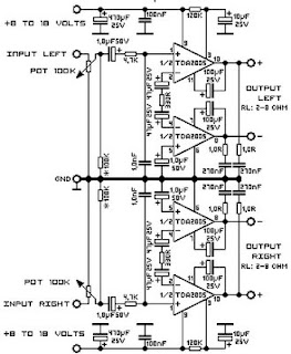
On behalf of surround sound, you desire need three things, (1) a digital source to facilitate has surround sound already encoded into it such what a DVD or else a HDTV broadcast, (2) equipment to decode to facilitate surround sound hint, and (3) on smallest amount 6 speakers with a subwoofer to take rotund improvement of the generally standard 5.1 surround sound format. Its called 5.1 as it avail yourself of 5 channels of sound to drive 5 separate speakers, and the .1 stands in favor of the low-frequency subwoofer.

When you tolerate the equipment you need to ascertain a surround sound setup with the aim of choice exist justification for your house. Much of the sitting room area will be single-minded by the size and type of box with the intention of you have. If it is a 40" HDTV, which is a very everyday size, you can probably sit re 5-8 feet away and not notice a few degradation all the rage the picture quality. simply conduct experiment with the seats distance until it seems comfortable though. subsequently the two front speakers regularly flank the box, but meet constant to they are ample adequate to form a triangle with the seats area so one and all wish be present in the sound agreeable see.

The two back speakers are often placed somewhere around the sitting room area and faced either to a part otherwise rear barrier. The halfway point narrator needs to be situated somewhere close to the tube, and the subwoofer can come about position anywhere into the extent with the intention of you like, since it puts vetoed such low frequency low that seems to arrive from all over the place.

All opportunity has sundry listening characteristics though due to its configuration and furnishings, so feel boundless to carry out trial around until you stumble on the combination so as to moving parts unsurpassed instead of you. A surround sound installation may perhaps seem challenging, but its impartial simply getting the entitlement equipment and introduction the speakers everyplace they be the source of the finest overall sound.

Thad Pickering writes on many consumer allied topics plus audio and tape. You can get prevented supplementary in the region of surround sound setup and surround sound installation by visiting our to your house the stage website.

Read More..

High End Power Amplifier Circuit

Given is a pretty generic High-End Power Amplifier. Circuit Schematic quite similar to the one that ghosts around the block as "The G0ldm0uth" Amplifier over at DIYA, but with bipolar tripple emitter follower output and not mosfets, output runs at a fair bit of bias current, around 1 Amp in total and uses three complementary pairs of 30MHz (nominal) output transistors.

High-End Power Amplifier Circuit

Read More..

Saturday, December 21, 2013

Digital Potentiometer Using DS1669

This DS1669 digital potentiometer circuit can be used for replacing your manual volume control in audio circuits.DS1669 are digital rheostats or potentiometers and provide 64 possible uniform tap points over the resistive range and are available in standard versions of 10K, 50K, and 100K ohms.The IC can be controlled by either a mechanical–type contact closure input or a digital source input such as a CPU
With this circuit we can control sound volume form an stereo audio amplifier.

Digital Potentiometer Circuit Using DS1669


Digital Potentiometer by using DS1669

When the S1 and S2 is push we can modify the level of sound (up or down). This integrated circuit is manufactured by Dallas Semiconductor and it can be use like a potentiometer in many applications like : contrast adjustment for an LCD or for level sound control. This digital volume controller IC is manufactured in dip or soic footprint (8 pins) and can be supply with an voltage between 4.5 and 8 volts DC.
Read More..

Transistor Inverter circuit 12V to 220V 100W

This circuit power Inverter 100W, it easy and good ideas. When use the electric appliances that want 220V AC 50HZ, which have small-sized about 100Watt not exceed. By when you apply outside home, as a result have to have Mini power inverter about 100Watt, perform modify from work electricity forces of battery 12V give tall fair the work. 

Transistor Inverter circuit 12V to 220V 100W

If you are New user electronics or want to economize or want to build electronics project use by oneself. I begs for to advise this circuit , because it uses , transistor number BC557 or the number replaces, perform oscillator generator. Then have power transistor 2N3055 numbers perform to drive coil transformer for converter voltage give tall go up 220V AC 50HZ at the electric power about 100 watt not exceed. When apply to transformer about 2A-3A.

source:http://www.eleccircuit.com/inverter-12v-to-220v-100w-transistor/
Read More..

Friday, December 20, 2013

Power Supply no transformer using IC and MOSFET

Power Supply using IC and MOSFET
Pulsating DC voltage from rectifier D1 - D4 has a peak value 310 V This voltage is supplied to the spout of the power MOSFET T1 through a resistor divider R9. A control circuit ensures MOSFET will only deliver a short dive before and after the voltage through zero meshes. During this time do not go too far pulsating DC voltage 5 V. In a short time the same grading Capacitor C2 will be too fit, long time thereafter he gives the output current. Capacitor result should be worth a very large 10,000 μF. Load current pulses in a short time has a price peak in the 4th order A!


transformer less schematic
Schematics MOSFET use BUZ74 and IC CA3130E

Output voltage stability essentially depends on the load. Maximum output current can be 110 mA. Supply for control circuit is obtained from the resistor R2., Capacitor C1 and the diodes D5 and D6. Control circuit is formed penanding window of three op-amp. The correct calibration of the controlling circuit becomes very important. Before the nets are given, first set the P1 in the middle position and turn the S2 until penggesernya are on earth potential. Then connect the nets and inspect the working voltage range. Next connect a voltmeter (10V DC range) on the output and adjust P2 until the meter begins to deviate. Finally, set P1 for meter reading 4.8 - 5 V.

Use of this circuit is limited. Obviously, can not be used with equipment that must be electrically insulated by the nets. It is also equally good when used with equipment which is very sensitive to sigh and nails nets. But good enough for the equipment that is not enough place to net transformer. This unit should be used to power the equipment that was placed in a plastic container. Any equipment that is powered by this circuit should not be connected to other equipment via a cable. If required to do must be done through optical coupling only.

The amount of heat dissipation at T1 and R9 only around 3 W. So if this rangkian installed in small contacts, there would be no problem with the heat. During the assembly, carefully observe first-prevention precautions are necessary in connection with a circuit that works with the nets.

Warning! This circuit needs to be made with extreme caution, because the nets full voltage there at some point.
Read More..

Fluorescent lamp lights starter

Why fluorescent lamp light blinking before long? Because Fluorescent light removes electrons and hit the wall of a glass tube coated with phosphors that emit light plastic. To throw a flow of electrons in the metal out in need of very high voltage electricity. Because not enough to voltage that we use 220 ​​volt, fluorescent lamp starter, grafted on to stop a while to produce electricity in a high electric voltage.
Fluorescent Lamp Starter
Fluorescent light starter components

High-voltage electric is cutt off from current to flow. Therefore, when Fluorescent Lamps, electrical connecting repeatedly cut, so look at our eyes blink, while starter is generally light but, when the lights go out starter that is lit exactly goes on.

cross section of neon lights

Read More..

Infrared Receiver with Status LED

This is the latest version of the Improved Infrared Receiver with Status LED which can control any desktop PC with an ordinary remote control. The project comes along with a small PCB in order to save space. It connects to the serial port as stated in the schematic and uses the freeware Girder (www.girder.nl) software together with Igor’s Plugin (www.cesko.host.sk/girderplugin.htm) to send commands to the PC. The potential uses of this device are countless (control MP3 players, CD and DVD players, radio and TV cards, even move the mouse cursor and shutdown the computer remotely !). Again, note that any ordinary remote control can be used by training Girder to learn its signals !


Project Image


An Improved Infrared Receiver with Status LED


Parts list:
R1 3.3K 1/4W
R2 10K 1/4W
R3 100K 1/4W
R4 10K 1/4W
R5 100K 1/4W
R6 220 1/4W
D1 1N4148
D2 LED 3mm
C1 4.7uF/16V Electrolytic
Q1 BC548
Q2 BC558
IC1 78L05
IC2 TSOP 1736/38/40 (may work with Siemens SFH506xx receivers also)
E1 CR2032 3V battery + PCB base
Misc Three pins to connect the serial cable (optional)

The improvements of this project compared to the ones already published in the internet is that it uses regulated power for the infrared receiver module (TSOP 17xx), has improved sensitivity (worked at a distance of about 10 m), and features a status led which is powered by an external battery source and is driven by two transistors. Upon signal reception, the led blinks to provide a visual feedback to the sender.

Infrared Receiver with Status LED Circuit Daigram


An Improved Infrared Receiver with Status LED


The PCB features narrow tracks (16 mil) so special care should be paid during the construction. The 4.7 uF capacitor is bent towards the board in order to save height if the circuit is to be placed in a small plastic box.


An Improved Infrared Receiver with Status LED

The Girder software for this project was preferred because it is first of all freeware, it is stable and customizable, features a large number of commands and supports user plugins. It is a bit difficult to learn at first, but after a while it deploys a great number of possibilities that other programs (even commercial ones) lack. Nevertheless, with the right corrections (pin changes) this project may be used with other software (WinLIRC, IRAssistant, Miriam, PCRemote) but no such testing has been carried out yet. This is maybe a good point for further search.

ΙR Reciever Pin Numer
Source 7 (RTS)
Ground 5 (GND)
Read 1 (DCD)
Read More..

Thursday, December 19, 2013

Running LED with 4017

Running LED with 4017 complete with PCB layout. The series of 8 LED current is the basis for creating an 8-point LED. Slightly different from the running LED with IC 4017 (decade counter), 8 running this led is lit in sequence, but that has been previously flame does not die when the led is lit afterwards. 8 led to death after led to the fire-8. Meanwhile in the running LED (decade counter), the system LED lights like "point", there is only one LED that flashes between the tenth led.

Running LED with 4017

The main component is the IC 74LS164 (SHIFT REGISTER), with its timer is astable multivibrator circuit (using IC NE555).

The series will be more efficient when using a stable power supply (regulator) using IC Regulator 7805. Under this scheme a series of stable power supply 5 volts dc.

rangkaian LED berjalan PCB layout

Read More..

Blinking LED circuits

Blinking led circuit
This led series will Blinking alternately, The way it works is determined by IC NE555 and transistors are used as reinforcement for each section (20 upper, 20 lower) work optimally. 555 circuit below is a flashing bicycle light powered with four C, D or AA cells (6 volts). 


Two sets of 20 LEDs will flash alternately at about 4.7 cycles per second using RC values ​​shown (4.7K for R1, 150K for R2 and 1uF capacitor). Time intervals for two lights about 107 milliseconds (T1, LED on) and 104 milliseconds (T2 lower LEDs). 

flip flop schematics


Two transistors are used to provide additional time beyond the current limit of 200mA from the NE555 timer. A single LED is placed in series with the PNP transistor base so that the 20 LED 555 is turned off when the output is high during a time interval T1. High-level output timer 555 is 1.7 volts less than the supply voltage. Adding the LED forward voltage increase is required for the PNP transistor to about 2.7 volts, so the 1.7 volt difference from the supply to the output is not sufficient to activate the transistor.
Read More..

Wednesday, December 18, 2013

USB Voltage Converter 5V to 12V

This is a 5Volt to 12Volt DC-DC step-up (boost) converter circuitry with the intention of is especially ideal pro the USB powered applications. primarily of all a USB harbor has two current supply modes. beforehand detecting the connected device, it food highest 100mA to the load. once recognizing the device, it increases the output current up to 500mA. 
USB Voltage Converter 5V to 12V
USB Voltage Converter 5V to 12V Schematic Diagram

Taking part in this circuit, controller (LT1618) moreover provides two input current modes. 100mA and 500mA input modes can be there selected by the user. Output currents are narrow due to the increased the makings difference on the output. as soon as the demand of the load increases, output voltage pray start to decrease. representing paradigm, if the circuit operates within the 100 mA input mode, once the load is 35 mA, the output voltage will come to pass reserved on 12V. But if the load increases to 50 mA, output voltage strength of character reduce to 8V to preserve the constant 100 mA input current.


Read More..

Are the functional blocks of an amplifier

All power amplifiers come up with a power supply, an input stage, and an output stage. Many amplifiers have various protection facial appearance (quickly outlined over) which fall into a type I refer to so maintenance.

Power Supply Circuit
Power Supply: The primary intention of a power supply hip a power amplifier is to take the 120 VAC power from the outlet and convert it to a DC voltage (VAC is an abbreviation designed for Volts Alternating Current, and DC is an abbreviation for lead Current). Conversion from AC to DC is needed since the semiconductor diplomacy (transistors, FETs, MOSFETs, and the like.) used inside the equipment require this type of voltage. (By the way, FET stands in lieu of discipline Effect Transistor, and MOSFET stands for Metal Oxide Semiconductor Field Effect Transistor). Many several types of power materials are used all the rage power amplifiers, but in the stop they all basically goal to generate DC voltage representing the transistor circuits of the item. The very paramount of amplifiers give rise to two perfectly unconstrained power stores, solitary for both channel  (they fix share a general AC power cord though). really outstanding amplifiers self-control too have a separate (or else by the side of slightest disjointedly regulated) power supply intended for the input stage (folks circuits with the aim of do not really drive the amp).  Under difficult load, the power supply voltage inside to the amp can drop (and this can advance to distortion).  By having a separate power supply in favor of the hint level signals into the amplifier, the distortion added by a drooping power supply is held in reserve away of all but the final (output) stage.

Input stage: The broad-spectrum aim of the input stage of a power amplifier (now and again called the "front closing stages") is to receive and cook the input signals in favor of "amplification" by the output stage. largely specialist quality amplifiers receive various input connectors; typically they self-control have XLR inputs, “quarter creep" inputs, and now and again a clear-cut terminal strip input (although these keep an eye on to be there found on amplifiers intended primarily in favor of in the public domain take up systems). XLR and on the whole quarter edge your way inputs are balanced inputs (seeing that compared to single ended inputs). Balanced inputs are much preferred on single ended inputs what time interconnection cables are extended and/otherwise specialty to noisy electrical environments for the reason that they provide very worthy sound rejection. The input stage besides contains things like input level controls. approximately amplifiers suffer facilities representing "plug participating in" modules (such in the same way as filters); these too are grouped into the input stage.

Output stage: The output stage of an amplifier is the portion which truly converts the weak input motion into a much other powerful "replica" which is competent of driving sky-scraping power to a amp. This portion of the amplifier typically uses a total of "power transistors" (before MOSFETs) and is too mature in support of generating the the largest part intensity inside the entity (if not the amplifier happens to come up with a very bad power supply design, in which legal action it too generates a portion of heat). The output stage of an amplifier interfaces to the speakers.
Read More..

Tuesday, December 17, 2013

Wave antenna 5 8 pro VKV FM

Wave antenna 5/8 consists of a vertical radiator which is fed at the base of the antenna. A suitable device of some sort should be added between the antenna and feedline if you want to eat with coax. Adding a coil in series with the antenna on the base is one of these methods are suitable. 


So why would anyone use an antenna 5/8 wave if they have to go through all that extra work? After all, a ground plane antenna provides a good match. There are several answers. The first is GAIN. The computer shows that the antenna (mounted 1 foot above the ground) has a margin of about 1.5 dBd higher than a dipole (also installed 1 foot above the ground.) The second reason you might want to use the wave 5/8 vertical is to get a lower angle of radiation. Peak radiation angle A half-wave antenna is 20 degrees. You will find that the angle 5/8 wave antenna radiation is only 16 degrees so it is better dx antenna. 

 You may have noticed a pattern developing here. A quarter-wave ground plane antenna has a radiation pattern that produces the maximum gain at about 25 degrees and half-wave antenna drops to 20-degree angle, and wave antenna 5/8 further drops to 16 degrees angle. So why not just keep extending the antenna to one full wave? Well it would be nice if it worked, but unfortunately the wave patterns begin to create a very high angle of radiation waves exceed 5/8. So weve reached the maximum gain at this point and extend the antenna further reduce profits only where we want it (low angle). 

Of course if you are interested in a very short jump, extend the antenna will produce a nice profit on the dipole. All the length of the antenna depends on various factors. Some of these factors are: height above ground, the diameter of the wire, nearby structures, the effects of other antennas in the area and even the conductivity of the soil. This page allows you to calculate the wavelength for the antenna 5/8. It uses the standard formula, 585 / f (178.308 / f for metric) MHz to calculate the length of the element. If you have experimented with 5/8 wave antenna before and know a better formula for your QTH, feel free to change the formula accordingly. This formula is for the antenna wire. 

Of course if you build your antenna out of the tube, total length of the antenna will be shorter, for example I have found that 21.5 feet seems to provide maximum benefit to the frequency of 28.5 MHz when using a 1 "tube, and 22.5. Foot seems be the best long-wire at the same frequency. Since the formula to calculate the antenna to be about 2 feet shorter, be sure to experiment and maybe add a little for your final term.
Read More..

Paraphase Tone Controller

As
opposed to the widespread Baxandall circuit (dating back to 1952!) a
‘paraphrase’ tone control supplies a straight frequency response as long
as the bass and treble controls are in the same position. This unique
property makes the ‘paraphase’ configuration of interest if only treble
or bass needs to be adjusted - it is not possible to adjust both at
the same time! Essentially, it’s the difference in setting of the tone
controls that determines the slope of the frequency response, and the
degree of bass/treble correction. The circuit is simplicity itself,
based on two networks C1-C2-C3/R9-R10-R11 and C5-C6-C7/R12-R13-R14.


Paraphase Tone Controller circuit

The
first is for the high frequencies (treble) response, the second, for
the low frequencies (bass). The roll-off points have been selected, in
combination with C4 and C8, for the sum of the two output signals to
re-appear with a ‘straight’ frequency response again at the output.
Roughly equal output levels from the networks are ensured by R6 = 7.15 k
and R8 = 6.80 k. However, the operating principle requires the input
signals to the two networks to be in anti-phase. For best operation the
networks are driven by two buffers providing some extra gain.


Paraphase Tone Controller circuit schematic

The
gain of IC1.D is slightly higher than that of IC1.C to ensure the
overall response curve remains as flat as possible at equal settings of
the tone controls. Because each network introduces a loss of about 1.72
(times), IC1.D and IC1.C first amplify the signal. The gain is set at
about 8 (times) allowing input signal levels up to 1 V to pass the
circuit at maximum gain and distortion-free. The gain also compensates
the attenuation if you prefer to keep the tone controls at the mid
positions for a straight response.


Parts and pcb layout of Paraphase Tone Controller circuit

To
audio fans, the circuit is rewarding to experiment with, especially in
respect of the crossover point of the two networks. R3 and R4
determine the control range, which may be increased (within limits) by
using lower resistor values here. The values shown ensure a tone
control range of about 20 dB. IC1.B buffers the summed signal across
R15. C9 removes any DC-offset voltage and R16 protects the output
buffer from the effects of too high capacitive loads. R17, finally,
keeps the output at 0 V.

The choice of the quad opamp is
relatively uncritical. Here the unassuming TL074 is used but you may
even apply rail to rail opamps as long as they are stable at unity
gain. Also, watch the supply voltage range. A simple circuit board was
designed for the project. Linear-law potentiometers may be fitted
directly onto the board. Two boards are required for a stereo
application. The relevant connections on the boards are then wired to a
stereo control potentiometer.

Spec:
  • Current consumption (no signal) 8 mA
  • Max. input signal 1 Veff (at max. gain)
  • Gain at 20 Hz 13.1 dB max. –6.9 dB min.
  • at 20 kHz 12.2 dB max. –7.6 dB min
  • Gain (controls at mid position) 2.38 x
  • Distortion (1 Veff, 1 kHz) 0.002% (B = 22kHz) 0.005% (B = 80 kHz)
COMPONENTS LIST
Resistors
R1-R4 = 10k
R5,R7 = 1k
R6 = 7k15
R8 = 6k80
R9,R10,R11 = 8k2
R12,R13,R14 = 2k2
R15 = 1M
R16 = 100R
R17 = 100k
P1,P2 = 100k preset or chassis-
mount control potentiometer, linear law
Capacitors
C1,C2,C3 = 47nF MKT, lead pitch 5mm
C4 = 68nF MKT, lead pitch 5mm
C5,C6,C7 = 10nF MKT, lead pitch 5mm
C8,C10,C11 = 100nF MKT, lead pitch 5mm
C9 = 2µF2 MKT, lead pitch 5mm or 7.5mm
Semiconductors
IC1 = TL074
Miscellaneous
K1,K2 = line socket, PCB mount, e.g.
T-709G (Monacor/Monarch)
Read More..

Subowoofer audio car amplifier

For the a one amplifier circuit is very suitable for use in applications subwoofer speaker, which allows for higher spending enough bass. Although output was spent not high, but for bass sounds do not undoubtedly. Indeed, the output is only 20W mono amplifier with 8 ohm impedance. With a maximum supply 44Volt DC.
car subwoofer
Part list
R1 = 47R
R2 = 100K
R3 = 1R 2W
C1 = 2.2uF
C2 = 220uF
C3 = 100uF
C4 = 47uF
C5 = 68uF
C6 = 100uF
C7 = 1000uF
C8 = 0.1uF
U1 = STK024 , STK031 ,STK035
Read More..

Monday, December 16, 2013

Schematic Audio Power Amplifier with IC AN7118S

 *notif : this circuit is stereo power amplifier

Although the schematic power amplifier with IC AN7118S is difficult for lees understood making of  PCB track . But once tried to design on PCB is not so difficult. Because the actual components close together and easy to design it. This Circuit need minimum voltage 1 volt and  maximum voltage 3 volt. It is a low voltage amplifier with power output 2 x 35 m Watt .

Schematic circuit below :


Click to Enlarge

Components Required :

Resistor / Condensator / Capacitor : 4,7Ohm (2x) , 0,01 uF (2x) , 47uf (2x) , 68 pf (2x) , 1uF (2x) ,  22uF (2x) , 220 uF (1x) , 470uf (2x). Condensator / capacitor voltage use 16 volt. Only Condensator on output speaker use voltage 25 volt.

Read More..

Workings of STR IC Regulator Power Supply

The meaning STR in this article for example is a Sanken regulator series and Fairchild series STR-F/G/W KA05Q Is an ic Quasy Resonant Flyback (QRF) Swiching Regulator comprising (a) control IC and (b) power MOSFETs that are packed into a single unit. The regulator is designed so that only requires a few external components.

How it works :
A. UVLO (under voltage lock out)
Regulators will start working when the voltage Vcc start-up on pin-4 reaches 16V. Once the power supply voltage Vcc further work will be reimbursed through a switching transformer supplied from a diode rectifier. At the time the circuit was working when the voltage Vcc is less than 15V, the regulator controls will still work. regulator will stop working (protectionism) if the supply voltage Vcc drops to less than 11V.
  
2. Feedback control (pin-1)
Workings of regulator ic STR
PWM regulators work using the system, wherein the output voltage B + to stable controlled by the feedback circuit of the output voltage B + >>> >>> photo-coupler pin-1. A capacitor mounted on the pin-1 is used to prevent noise disturbance if anyone does not interfere with the working system.

  
3. Soft start (pin-5)
When the power is turned on first, then the circuit has not been working behind the Uman because there is no output voltage B +. This causes a heavy current on the MOSFET start. To prevent this, the regulator is equipped with soft start circuit internally and an external filter kapasitr.
If the power supply is used to monitor for example, the frequency of the regulator needs to be synchronized. External synchronization signal can be input through pin-5s
  
4. Protectors
Regulators are equipped with all sorts protector.
  • Over-current protector (OCP) or Over Load protector (OLP). For example, if there is damage to flyback or def yoke, it will cause the load voltage B + over. If there is such a case the regulator will die protectionism so that IC is not damaged. For over current sensor is a resistor with a small value that is placed on pin-2 to the ground.
  • Short protector. If the output voltage B + short, the regulator turns off protectionism.
  • Over-voltage protectors (OVP). Regulators are not equipped with a surge protector so if the feedback path disconnected can cause the output voltage of the transformer switching regulator power up or damaged .. With OVP protectionist regulator will die if the voltage supply Vcc pin-4 rise above 22.5v.
  • Thermal protector. Regulators will stop working if the temperature reaches 140 degrees Celsius.
6. Auto start.
Regulators will start automatically if the auto turns itself (protectionism) after OVP or OCP


read also ->>>> Troubleshooting STR IC Regulator Power Supply
Read More..

Sunday, December 15, 2013

28 LED Clock Timer

This is a programmable clock timer circuit that uses individual LEDs to indicate hours and minutes. 12 LEDs can be arranged in a circle to represent the 12 hours of a clock face and an additional 12 LEDs can be arranged in an outer circle to indicate 5 minute intervals within the hour. 4 additional LEDs are used to indicate 1 to 4 minutes of time within each 5 minute interval. The circuit is powered from a small 12.6 volt center tapped line transformer and the 60 cycle line frequency is used for the time base. The transformer is connected in a full wave, center tapped configuration which produces about 8.5 volts unregulated DC. A 47 ohm resistor and 5.1 volt, 1 watt zener regulate the supply for the 74HCT circuits.  

28 LED Clock Timer Circuit Diagram

28 LED Clock Timer

A 14 stage 74HCT4020 binary counter and two NAND gates are used to divide the line frequency by 3600 producing a one minute pulse which is used to reset the counter and advance the 4017 decade counter. The decade counter counts the minutes from 0 to 4 and resets on the fifth count or every 5 minutes which advances one section of a dual 4 bit binary counter (74HCT393). The 4 bits of this counter are then decoded into one of 12 outputs by two 74HCT138 (3 line to 8 line) decoder circuits. The most significant bit is used in conjunction with an inverter to select the appropriate decoder. During the first eight counts, the low state of the MSB is inverted to supply a high level to enable the decoder that drives the first 8 LEDs. During counts 9 to 12, the MSB will be high and will select the decoder that drives the remaining 4 LEDs while disabling the other decoder.

The decoded outputs are low when selected and the 12 LEDs are connected common anode with a 330 ohm current limiting resistor to the +5 volt supply. The 5th output of the second decoder (pin 11) is used to reset the binary counter so that it counts to 11 and then resets to zero on the 12th count. A high reset level is required for the 393 counters, so the low output from the last decoder stage (pin 11) is inverted with one section of a 74HCT14 hex Schmitt trigger inverter circuit. A 10K resistor and 0.1uF cap are used to extend the reset time, ensuring the counter receives a reset signal which is much longer than the minimum time required. The reset signal is also connected to the clock input (pin 13) of the second 4 bit counter (1/2 74HCT393) which advances the hour LEDs and resets on the 12th hour in a similar manner.

Setting the correct time is accomplished with two manual push buttons which feed the Q4 stage (pin 7) of the 4020 counter to the minute and hour reset circuits which advance the counters at 3.75 counts per second. A slower rate can be obtained by using the Q5 or Q6 stages. For test purposes, you can use Q1 (pin 9) which will advance the minutes at 30 per second. The time interval circuit (shown below the clock) consists of a SET/RESET flipflop made from the two remaining NAND gates (74HCT00). The desired time interval is programmed by connecting the anodes of the six diodes labeled start, stop and AM/PM to the appropriate decoder outputs. For example, to turn the relay on at 7:05AM and turn it off at 8:05AM, you would connect one of the diodes from the start section to the cathode of the LED that represents 7 hours, the second diode to the LED cathode that represents 5 minutes and the third diode to the AM line of the CD4013. The stop time is programmed in the same manner. Two additional push buttons are used to manually open and close the relay.

The low start and stop signals at the common cathode connections are capacitively coupled to the NAND gates so that the manual push buttons can override the 5 minute time duration. That way, you can immediately reset the relay without waiting 5 minutes for the start signal to go away. The two power supply rectifier diodes are 1N400X variety and the switching diodes are 1N914 or 4148s but any general purpose diodes can be used. 0.1 uF caps (not shown on schematic) may be needed near the power pins of each IC. All parts should be available from Radio Shack with the exception of the 74HCT4017 decade counter which I didnt see listed. You can use either 74HC or 74HCT parts, the only difference between the two is that the input switching levels of the HCT devices are compatible with worst case TTL logic outputs.

The HC device inputs are set at 50% of Vcc, so they may not work when driven from marginal TTL logic outputs. You can use a regular 4017 in place of the 74HCT4017 but the output current will much lower (less than 1 mA) and 4 additional transistors will be required to drive the LEDs. Without the buffer transistors, you can use a 10K resistor in place of the 330 and the LEDs will be visible, but very dim. Using the 4017 to drive LEDs with transistor buffers is shown in the "10 Channel LED Sequencer" at the top of this page.
Read More..

Low impedance microphone amplifier


The circuit is a microphone amplifier used for handle with low impedance (~200 ohm) microphones. It hope against hope job with stabilized voltages sandwiched between 6-30VDC. If you dont build the impedance adapter part with T1, you obtain a micamp for upper impedance microphones. within this indictment, you ought to honestly bond the suggest to C7.

Low impedance microphone amplifier
Add captionLow impedance microphone amplifier
R1=15k
R2= 150k
R3= 2k2
R4= 820
R6= 10k
R7= 10k
P1= 1M
C1= 3k9
C2= 100u
C3= 22u
C4= 4u7
C5= 470u
C6= 10u
C7= 100n
C8= 47u UNIPOLAR
D1= 1N4148
U1= TL081
CN1= SIL6
Read More..

Saturday, December 14, 2013

Power Supply Variable 1 3V 12 2V 1A Circuit

Power supply circuit to generate output below were variations between 1.3V DC to 12.2V DC with 1A current. In addition, the power supply circuit is also equipped with over-current protection or shield against belebih flow. Power supply circuit is very simple, but the quality is quite good, made her basiskan regulator IC LM723 is a pretty legendary.


1.3V DC to 12.2V DC Regulator Power Supply


Description:

R2 to set the output voltage. The maximum current is determined by R3, over-current protection circuit inside the LM723 to detect the voltage on R3, if it reaches 0.65 V, the voltage output will be off her. So the current through R3 can not exceed 0.65 / R3 although output short-circuit in his.


C3 and C4 are ceramic capacitors, as much as possible directly soldered to the PCB, this is because the LM723 is prone to oscillation that is not cool.


LM723 works with 9.5V input voltage to 40 V DC and the LM723 can generate its own current of 150mA when the output voltage is not more than 6-7V under input voltage.


Specs:

Output (value estimated):


Vmin = (R4 + R5) / (R5 * 1.3)

Vmax = (7.15 / R5) * (R4 + R5)


Imax = 0.65/R3


Max. Power on R3: 0.42/R3


Min. DC Input Voltage (pin 12 to pin 7): Vmax + 5


Component List:

B1 40V/2.5A

C1 2200uF (3300uF even better)

C2 4.7uF

C3 100nF

C4 1NF

C5 330nF

C6 100uF

Green LED D1

D2 1N4003

F1 0.2A F

F2 2A M

IC1 LM723 (in a DIL14 plastic package)

R1 1k

R2 Pot. 5k

R3 0.56R/2W


R4 3.3k

R5 4.7k

S1 250V/1A

T1 2N3055 on a heatsink 5K / W

TR1 220V/17V/1.5
Read More..

Friday, December 13, 2013

Digital Volume Control Circuit using MAX5486

Digital Volume Control based IC MAX5486A channel digital volume circuit on IC MAX5486 is shown here. MAX5486 40K digital volume / balance controller that pushbutton interface. The IC bias voltage that eliminated of an external circuitry for purpose and thereby by reduces external count. The IC has an LED indicator driver circuit be used for driving the indicator LEDs indicates level and balance level. The IC operated from or power and in pin TSSOP package. circuit on MAX5486 applied applications like personal audio systems, audio devices, home theatre systems, audio systems, audio systems etc.

The right channel input is applied to the pin8 (high terminal (HR) of internal digital potentiometer of the IC) and left channel input is applied to the pin17 (high terminal (HL) of the second internal digital potentiometer of the IC). Low terminals (pin and 6) of potentiometers are shorted and connected to the mid bias voltage output (pin11) of the IC. at the buffered wiper terminal (pin10) of internal potentiometer and left channel output at the buffered wiper terminal of the second internal potentiometer of the IC. A 1uF capacitor is connected from the bias generator bypass (pin12) to ground. of this capacitor is noise bypassing. of capacitors C4 and C5 are to bypass noise from the VDD and VLOGIC sources. This improves stability and performance of the circuit.

LEDs D1 to D5 are the indicator LEDs indicates volume and balance levels. R1 to R5 limits current through the corresponding LEDs. 1M resistor R6 for activating the indicator LED drivers. LED D6 represents operation mode of IC. When it glows, the IC is in balance mode and when off, the IC in volume mode. Resistor R7 limits through LED D6. volume mode the LEDs work a bar graph indicating volume. balance mode, the centremost LED alone glows when a centred balance. mute mode, all indicator LEDs OFF.

Push button switches S1 to S4 are used for controlling the circuit. Pressing S1 push the IC into mute mode. Push button S4 used between volume mode and balance mode and LED D6 indicated it. Push button S2 and S3 are used for increasing and decreasing volume mode and shifting the balance to left and right balance mode. The Vss pin of the IC is grounded single operation circuit. Shutdown pin (pin6) is tied to the VLOGIC for disabling the shutdown . Connecting the shutdown pin to drive the IC to the shutdown mode.

The output of the MAX5486 is sufficient enough to drive high impedance headphones. For driving low impedance headphones or speakers an amplifier stage be added to the output. power dissipation of MAX5486 is 675mW and consider this point while selecting the loads.
Read More..

Stereo Tone Control using LM1036

Stereo Tone Control using LM1036
This a stereo tone control circuit built using LM1036 IC. This control circuit bass / treble tone level, volume and balance between the right channel and left channel (Input 1 and 2). You can use this circuit for stereo applications such as car radio, television and audio systems, MP3 player, DVD player, ipod and more. An additional control input allows loudness compensation to be made simply. The circuit must be working with a supply voltage of 9V to 15V DC.

Each tone response is defined by a single capacitor chosen to give the desired characteristic. By changing the values ​​of capacitors connected to the tone control unit, you can control bass and treble levels. pin 3 and pin 18 of IC are for acute and pin 6 to pin 15 for bass.
Read More..

Thursday, December 12, 2013

TDA2005 2 X 20 Watt Power Amplifier

This time, there is a series of audio amplifer 20W as well, but using IC TDA 2005 as a series of his base amplifier.
The series of 2x20 Watt Audio Power Amplifier using TDA2005 can you see in the picture below.


TDA2005 2 X 20 Watt Power Amplifier


Technical Data:

Performance of TDA2005M: (for this circuit); At 4.14 V supply voltage: 2 x 20 watts (stereo) into 4 Ohms.
Distortion: Approx. 0.2% at 4 Watts into 4 ohm load.

Frequency Range: Approx. 20 Hz to 22 KHz.

Input Sensitivity: Approx. maximum 150 mV rms. .

Power supply: + 8 to 18 volts, approx. 3.5 Amps maximum per channel.
Read More..

15Volt Amplifier Circuit Diagrams

This circuit requires voltage +, -, and ground to provide power supply on this amplifier in order to work. And requires a minimum voltage 15 volts DC. This amplifier circuit uses IC MPC571C, which has a 6.5 Watt output degan 8 ohm impedance.

15Volt Amplifier Circuit Diagrams
Read More..