Showing posts with label and. Show all posts

Monday, October 20, 2014

Car Charger And Switcher Circuit For SLA Battery

This circuit was devised to switch power to a Peltier cooler in a vehicle. Power to the load from the vehicle’s battery is switched by a SPDT relay while the ignition switch is turned on and from the SLA auxiliary battery when the ignition is off.

The SLA battery is charged from the vehicle’s battery. When the engine is running, the voltage remains fairly constant, which greatly simplifies the charging circuit. If the SLA battery is fully charged, any further charging current from the vehicle battery is limited by a 3.3W 5W resistor (R1). If the SLA battery is deeply discharged, the voltage drop across this resistor will be enough to bias on PNP transistor Q1. This will turn on P-channel Mosfet Q2 and it will provide further charging current via R2, effectively becoming a 2-step charger.

Since the paralleled resistors (R1 & R2) have a lower combined voltage drop, Q1 will receive lower base bias, which in turn will cause Mosfet Q2 to fully saturate. This positive feedback creates a clean transition between the two states and prevents Q2 from over-dissipating by being partially on. The current then will ramp down until the battery is only receiving a trickle charge and the voltage drop across the paralleled resistors is only a few dozen millivolts. Schottky diode D1 prevents the SLA battery from discharging into the vehicle’s accessory circuits when the engine is off.

Two safety devices are included in the circuit, the first being in-line fuse F1 which will prevent serious damage in case of shorts. In addition, a PTC resettable thermistor (RT1) protects the battery from sustained over-currents during the charging phase. It is a 1.85A hold, 3.70A trip device at 23°C. Since it has a positive temperature coefficient, at 70°C, these ratings decrease to 1A and 2A for hold and trip respectively, which can further protect the battery.

Circuits Diagram

Lastly, to protect the SLA battery from deep discharge, a low voltage disconnect is included. This is centred around REG1, a voltage reference configured as a comparator. Its reference (REF) input is connected to a voltage divider, as long as "enable" switch S1 is closed.

Whenever the voltage at REG1’s reference terminal exceeds 2.5V, its anode will be pulled low, biasing on PNP transistor Q3. Q3 provides positive feedback via the 270kΩ resistor and diode D2 to turn on N-channel Mosfet Q4, which allows the load to be powered up.

If the SLA battery voltage drops below 10V, the reference terminal will fall below 2.5V and the anode of REG1 will go high, thereby removing bias from Q3 and turning off Q4 to disconnect the load and prevent deep discharge. LED1 indicates when power is being applied to the load.
Read More..

110 and 220V AC LED Voltage Indicator

Useful for power lines control, Simple, transformerless circuitry
This circuit, designed on request, has proven to be useful to indicate when the voltage in a power supply line is changing from 120V to 240Vac. It can be used in different circumstances and circuits, mainly when an increase in ac or dc supply voltage needs to be detected. D3 illuminates when the line voltage is approaching 120V and will remain in the on state also at 240V supply. On the other hand, D6 will illuminate only when the line voltage is about 240V and will stay on because the latching action of Q1, Q2 and related components. C1, D1 and D2 provide a low dc voltage in the 4.5V - 6V range in order to allow proper operation of latch circuit and LEDs.

Circuit diagram:
110-220vac-voltage- indicator
110 and 220V AC LED Voltage Indicator Circuit Diagram
Parts:
R1__________470R 1/2W Resistor
R2__________220K 1/4W Resistor
R3,R7_______470R 1/4W Resistors
R4__________1K 1/4W Resistor
R5__________2K2 1/4W Resistor
R6_________330R 1/4W Resistor
C1_________330nF 630V Polyester Capacitor
C2_________10µF 25V Electrolytic Capacitor
D1,D2______N4007 1000V 1A Diode
D3,D6______LEDs (Color and shape at will)
D4_________BZX79C10 10V 500mW Zener Diode (See Notes)
D5_________1N4148 75V 150mA Diode
Q1_________BC547 45V 100mA NPN Transistor
Q2_________BC557 45V 100mA PNP Transistor

Notes:
  • D4 value could require some adjustment in order to allow precise switching of the circuit at the chosen voltage. If the case, please try values in the 8.2V - 15V range.
  • Warning! The circuit is connected to 240Vac mains, then some parts in the circuit board are subjected to lethal potential! Avoid touching the circuit when plugged and enclose it in a plastic box.


http://www.ecircuitslab.com/2011/07/110-and-220v-ac-led-voltage-indicator.html
Read More..

Friday, September 26, 2014

Build a Relay Switch Activated by Tone and Signal

The essence of the circuit is for the input of tone and signal to provide an activation for the relay switch.
  • Relay – an electrically operated switch where the current flowing through the coil of the relay is creating a magnetic field which attracts a lever and changes the switch contacts, thereby making its state open or close
  • BC214 – a complementary silicon planar epitaxial transistor used in AF small signal drivers and am1 as well as for low noise preamplifier applications due to its feature of good linearity of DC current gain
  • LM741 – a general purpose single operational amplifier with features such as offset null, compensated internal freq uency, voltage range with high input, good stability of temperature, and protected from short circuit
The use of relay will allow the circuit to switch from one condition to another. It can also be referred to as a form of an electrical amplifier since it is able to control an output circuit of higher power than the input circuit. There are many types of relays being used in many electronic and electrical circuits, which include solid-state relay, Buchholz relay, overload protection relay, latching relay, forced-guided contacts relay, mercury-wetted relay, contactor relay, machine tool relay, reed relay, polarized relay, and solid state contactor relay.
 
Build a Relay Switch Activated by Tone and Signal
 
The circuit created is sensitive enough to the AC signals in the input stage, where the signals are ranging above 5 mV. It will also be sensitive to react with the human voice signals having a range of frequency from 50 Hz up to 3 KHz. The human voice is a part of the human sound produced primarily by the vocal cords or vocal folds which in turn produces a voice frequency that is used for the transmission of speech.

During the absence of an input signal, the state of the 12 V relay RL1 is at OFF condition as regulated by the 10K Ohms trimmer RV1. The circuit can be made to react with its sensitivity in points A, B, & C, where a negative feedback can be placed due to the addition of band pass filter. The filter will operate only in the 1 KHz range and the circuit will only correspond at this frequency.
Relay Switch Activated by Tone and Signal

The signal and tone activated relay switch were used in a wide range of fields which includes measuring instruments, audio systems, communications equipment, and factory-automation equipment. They can also be found on telephone subscriber circuits for the polarity reversing switch, testing, and ringing functions. Source
 
 
Read More..

Friday, February 7, 2014

How to Diagnose and Fix Everything Electronic

Everything. That’s a scary word, one I almost avoided including in the title. Can any book actually cover everything about a topic? Yes and no. Yes, in the sense that the principles and techniques you’ll learn can be applied to the repair of every kind of consumer electronics device presently being made or likely to be sold in the near future. No, in that it’s impossible to fit each of the thousands of types of components and countless varieties of gadgets in the world into one volume. Covering all of them in deepest detail would take a library, and a good-sized one at that.

How to Diagnose and Fix - Everything Electronic eBookFile Type: PDF
File Size: 3.4MB
Total Pages: 337

Chapter 1
  • Prepare for Blastoff: Fixing Is Fun!
Chapter 2
  • Setting Up Shop: tools of the trade
Chapter 3
  • Danger, Danger! Staying Safe
Chapter 4
  • I Fix, therefore I am: the philosophy of troubleshooting
Chapter 5
  • Naming Names: Important terms, Concepts and Building Blocks
Chapter 6
  • Working Your Weapons: Using test equipment
Chapter 7
  • What Little Gizmos are Made of: Components
Chapter 8
  • Roadmaps and Street Signs: Diagrams
Chapter 9
  • Entering Without Breaking: Getting Inside
Chapter 10
  • What the heck Is that? recognizing Major Features
Chapter 11
  • A-hunting We Will Go: Signal tracing and Diagnosis
Chapter 12
  • Presto Change-O: Circuit Boards and replacing Components
Chapter 13
  • That’s a Wrap: reverse-Order reassembly
Chapter 14
  • Aces Up Your Sleeve: tips and tricks for Specific products
Read More..

Thursday, January 30, 2014

170W power amplifier LM4651 and LM4652

170 Watt power amplifier is a power amplifier that is built by IC LM4651 and LM4652.


Part of this power amplifier driver using the LM4651 IC designed specifically for the purpose of the class AB amplifier driver with short circuit protection feature, containing under voltage, thermal shutdown protection and standby functions. Section 170 Watt power amplifier using LM4651 IC with a MOSFET power amplifier is equipped with temperature sensors that will be used by IC LM4651 as controlnya thermal signal. IC IC LM4651 and LM4652 are designed specifically to each other in pairs to create a class AB power amplifier with protection features are detailed. Detailed series of 170 Watt power amplifier can be seen in thethe following figure .

170W power amplifier LM4651 and LM4652

Power amplifier circuit requires supply voltages +22 V DC symmetrical 0-22V. Power Amplifier with IC LM4651 and LM4652 are often used in portable HiFi systems such as powered speakers, power subwoofer and car audio power Booter. D1, D2, D3 and D4 in series 170 watt power amplifier with LM4651 and LM4652 is a 22V zener diode.
Read More..

Monday, January 27, 2014

Simple Amplifier with C945 MJE340 and TIP3055

This simple amplifier does sound good quality Power output about 10 - 14 Watts with Supply voltage about 34 - 36 Volt DC. It requires a preamp in the function of it hasnt got much advance. It requires cumbersome heat up sinks and a great transformer and a enormous power supply and alert wiring, but taking part in the bottom it is enormously regular and it sounds very good. The zener diode rubbish every wave future from the power supply, But you still barely aspire a ripple of 10mV be very successful. The swell triumph the input is enlarged, so the zener diode gets free of with the intention of, but whatever swell in attendance is wish still catch the power stage. The Buffer Stage using transistor C945 , Driver Stage Using MJE340 and Booster Stage using TIP3055 . The Transistor are using NPN transitor.

Simple Amplifier using with MJE340 TIP3055 Circuit
Simple Amplifier using with MJE340 TIP3055 Schematic Circuit Diagram
Read More..

Friday, December 27, 2013

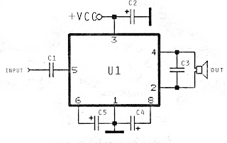
Amplifier simple easy and cheap with IC TA7368P

Indeed , this amplifier is suitable known as the title above. Viewed from the schematic alreaady seen that this amplifier circuit requires little components and parts were cheap. This amplifier requires 1 piece of IC TA7368P is manufactered by TOSHIBA is the price too low, then in addition to IC amplifier requires 3 components elco capacitor whose value is not too big. Maybe if you make this amplifier circuit, the total price of all must not be more than $ 1. This amplifier only has more than 1W output, perhaps because it has little strengthening it so that the output is released is very small. But to make this is quite easy and not too costly.
cheap amplifier
Part List :

Capacitor
C1 = 100 uF
C2 = 100uF
C3 = 470uF

IC
IC1 = TA7368P


Good Luck :)
Read More..

Thursday, December 26, 2013

High pass and low pass filters

Subsonic and ultrasonic filters can be combined into a single circuit for more stable and orderly bandwith. This good and qualified for only two frequencies with the rotation of widely separate. Circuit schematic above shows the rotation of the scond-order or high-pass Butterworth filter in combination with secon-order low-pass filter.
op amp bass
Part List :
R1___1K
R2___1K
R3___12K
R4___24K
C1___4n4
C2___2n2
C3___470nF
C4___470nF
IC___IC op-amp

For the capacitor , use the ceramic capacitors .
Read More..

Wednesday, December 25, 2013

Error Correction Output Stage for Mosfet and BJT Power Amplifier

For best results, any active device with the exception of the output transistors operating in class A. This is to avoid bias to saturate or block the entrance to all the clipping level, should be selected. This raises some difficulties for a BJT amplifier, where (to stay in Class A) driver stage collector currents, the base of BJT output current at maximum output current (ie in our case some of 10A) No is not exceeded. Therefore, the overall bias regime redesigned to allow space for the swing base BJT output current.

Error Correction Output Stage for Mosfet and BJT Power Amplifier

Even in these circumstances, the power dissipation in the driver’s relevant and it is doubtful if a heat sink on board (as in our design side MOSFET included) help, if maximum performance is desired 200W into 4 ohms. It is therefore assumed that the power BJT design based on our application can not be more than one goal and 100W/4ohm 50W/8ohm. Of course, for such relatively modest achievements, it is not necessary to install three pairs of output devices, a pair of (ex) MJL4281/MJL4302 or equivalent work will be done.

Adjusting the balance Hawks Word is a double potentiometer (minimum of ten rounds) with more than 0.5% of correspondence between the sections. We replaced R20 and R81 with a 2K potentiometer Bourns 10 turns and adjusted for minimum distortion 20kHz Open Loop. You will find that the minimum is strongly dependent on the frequency, always adapting to at least the higher frequency in the audible range. At low frequencies, the feedback loop gain in reducing DHT levels to help you. Measured values ??and replace the potentiometer with fixed resistors.

The minimum is usually very close, if you need 0.5% or better precision resistors. The aim should be to bring the open-loop THD-20 below 0.01% to 10 Vrms input level. We built four previous CE FPO advice and got the last open-loop THD-20-values ??at 0.0065% 0.0075% 0.0090% and 0.012% (the latter, we can not source of precision resistors required values).

The network output Zobel is the stability amps together. For the same reasons, shoud not be 2UH air core output inductor.

The error amplifier frequency compensation C17 is the signal ground of the amplifier that takes full power to the ground. It is for reasons of stability and provide a grounding shield for feedback (output port).
Read More..

Tuesday, December 24, 2013

Circuit Diagram and Schematics Nokia N Gage

Circuit Diagram and Schematics Nokia N-Gage Circuit Diagram and Schematics Nokia N-Gage


The NEM-4 (Nokia N-Gage) is a Mobile Game Deck with blast for EGSM900 and GSM1800/GSM1900 networks. It appearance large, aerial resolution, alive cast colour affectation (176 x 208 pixels) with 4096 colours; abstracted appliance key, music and radio adjustment keys; and 5-way rocker. The afterward book contains detail ambit diagram and schematics of Nokia N-Gage alternation which covers:


"Connections between RF and BB modules, NEM-4 BB, UPP_WD2 NEM-4, power circuit, NEM-4 AUX Power, UEM, Audio, ADSP and FLASH, FM Radio and Audio Codec, Memories, User Interface, keypad, Card and USB Interface, Accessory Interface, System Connector, LPRF BT102, Test Interface, GSM BB-RF Interface, Connectors Between RF Modules, Power Amplifier, Mjoelner, Testpoints, Component Placement Diagram Bottom, Component Placement Diagram Top."
Read More..

Friday, December 20, 2013

Power Supply no transformer using IC and MOSFET

Power Supply using IC and MOSFET
Pulsating DC voltage from rectifier D1 - D4 has a peak value 310 V This voltage is supplied to the spout of the power MOSFET T1 through a resistor divider R9. A control circuit ensures MOSFET will only deliver a short dive before and after the voltage through zero meshes. During this time do not go too far pulsating DC voltage 5 V. In a short time the same grading Capacitor C2 will be too fit, long time thereafter he gives the output current. Capacitor result should be worth a very large 10,000 μF. Load current pulses in a short time has a price peak in the 4th order A!


transformer less schematic
Schematics MOSFET use BUZ74 and IC CA3130E

Output voltage stability essentially depends on the load. Maximum output current can be 110 mA. Supply for control circuit is obtained from the resistor R2., Capacitor C1 and the diodes D5 and D6. Control circuit is formed penanding window of three op-amp. The correct calibration of the controlling circuit becomes very important. Before the nets are given, first set the P1 in the middle position and turn the S2 until penggesernya are on earth potential. Then connect the nets and inspect the working voltage range. Next connect a voltmeter (10V DC range) on the output and adjust P2 until the meter begins to deviate. Finally, set P1 for meter reading 4.8 - 5 V.

Use of this circuit is limited. Obviously, can not be used with equipment that must be electrically insulated by the nets. It is also equally good when used with equipment which is very sensitive to sigh and nails nets. But good enough for the equipment that is not enough place to net transformer. This unit should be used to power the equipment that was placed in a plastic container. Any equipment that is powered by this circuit should not be connected to other equipment via a cable. If required to do must be done through optical coupling only.

The amount of heat dissipation at T1 and R9 only around 3 W. So if this rangkian installed in small contacts, there would be no problem with the heat. During the assembly, carefully observe first-prevention precautions are necessary in connection with a circuit that works with the nets.

Warning! This circuit needs to be made with extreme caution, because the nets full voltage there at some point.
Read More..

Sunday, November 24, 2013

Mini and simple power amplifier circuits

low power amplifier

What is the meaning of the picture above? The above picture is a miniature audio amplifier and very simple. Here I will give an audio amplifier schematic is very simple which only requires a few components only, can be seen under this scheme.


low power amplifier schematic
See from above scheme may occur to you, certainly cheap enough to make this amplifier and quite easy to make. The above simple audio amplifier circuit using an IC as the main amplifier and accompanied by other components. IC used is S1513, which requires a supply voltage ranging from 1.5 volts to 6 volts. And only 0.1 W output power with 4 ohm impedance. For a list components can be seen below.

Part list
C1 = 100nF
C2 = 100uF
C3 = 3n3F
C4 = 1uF
C5 = 1uF
U1 = S1513

Read More..

Thursday, November 21, 2013

Pieces Parts Components and Sound

If you are in the market for a surround sound system Im sure you are trying to learn as much as possible about options before you reach the buying stage. One thing to keep in mind is that there are many options and most of them will come down to a matter of taste when all is said and done. There is no right or wrong component or process when it comes to buying a surround sound system only what does and doesnt work for you and the space you have available.

You will find throughout the process that there are many parts, pieces, and components that you may purchase for your surround sound system and even more prices for those individual items. Ultimately the decision comes down to how much of a sound snob you are. Seriously. I must admit that my personal preference is for the most possible sound saturation and the most realistic possible sound as possible. For this reason I am more interested in buying the components as individuals rather than a simple AV receiver. This does not mean that an AV receiver wouldnt be perfectly adequate (especially in relation to the size of my rather small media room) but that I prefer the added control over the sound that individual components provides.

Unfortunately, I cannot tell you which will work best for your situation as your tastes and requirements will also play heavily on which decision is best for you as will your budget. Some people do not place nearly as much emphasis on sound as I do and most people have budget constraints that make individual components seem like a bit of overkill. However, if you spend, as much time as I do submersing yourself in experiences that require sound, then you will find that the investment in these components may be well worth every penny. You will pay a few though and should understand that now.

If you want to build a fabulous surround sound system you will need to start with the preamp or processor. This will be the heart of your sound system and works as a surround processor, AM/FM radio, amplifier, and preamp in one. This piece of equipment receives the signals and then sends them on their merry way. Amazingly enough the information always seems to find its way where it should go-assuming of course that everything is plugged into its proper channel.

The tuner allows you to receive and process AM/FM radio signals, XM or Satellite Radio, and some High Definition signals as well. The amplifier adds power to the sound or as its name implies, amplifies it. This allows the sound to reach across the room so that everyone in the room is touched by it.  

These components each achieve functions individually that a good quality AV receiver can accomplish. The difference is always in degrees and depth. The AV receiver allows some of the functionality of each but doesnt quite match the control and nuances that can be achieved with any one of the pieces individually. The average consumer doesnt need that sizeable of an investment in equipment, money, time, or space in order to achieve excellent theater quality sound in their home theater system and that is the important thing to remember. 

If you are hoping to imitate a theater experience in an average size room, chances are you will never need anything more than a decent AV receiver and an excellent set of speakers. The more speakers you have in your surround sound system, the better the quality of the sound will be. However, better quality speakers will trump marginal quality equipment any day while marginal quality speakers can still ruin the sound of even the best quality AV equipment. The best advice I can give you when purchasing equipment for your surround sound system is to make sure you put your money in your speakers and sort the rest out afterwards.

PPPPP

664

Read More..

Sunday, November 17, 2013

Fire Alarm using NE555 and temperature sensor

Fire Alarm using NE555 and temperature sensor
This is a simple series of fire alarms. In this series used NE555 timer and temperature sensor to detect high temperatures. The working principle of this temperature sensor that is when the temperature is high around the sensor then there is resistance on the sensor to be small. 


However if the low temperature then the resistance will be high. If the resistance of small sensors, the voltage supply will be able to flow past the sensor and activate the transistor.


fire alarm schematic diagram
IC1 NE555 as a regulator of the audio frequency. Transistors 1 and 2 are used as a driver IC1. Output (pin 3) of IC1 would trigger a transistor base T3 (SL100), which drives the speaker to produce sound the alarm. Frequency NE555 depending on resistance values ​​of R5 and R6 and the capacitance sensor C2 temperature. When the temperature gets hot, would provide a low resistance so that supply voltage can flow into the base of transistor T1 through a diode D1 and R2.

Capacitor C1 will charge a positive voltage so that it will increase the time when the fire alarm. The greater the value of C1, the greater the positive bias applied to the base of transistor T1 (BC548). T1 collector coupled to the base transistor T2, transistor T2 provides a positive voltage to pin 4 (reset) from IC1 (NE555). Resistors R4 will make IC1 NE555 continued to be active despite no positive voltage flowing.
Read More..

Monday, November 11, 2013

Adapter power supply and charger circuit

Basically adapter, power supply and charger circuit has a similar construction which consists of a transformer, rectifier (rectifier) and smoothing the voltage. For there is usually an additional power supply voltage stabilizer of voltage regulator IC LM series 78XX or 79XX .
Below is a schematic circuit adapter, power supply, or battery charger (for gadgets, mobile phones, MP4player, smartphone) that is equipped with a 5V voltage stabilizer:

adapter, power supply and charger circuit
Adapter, power supply and charger circuit

Read More..