his circuit provides a simple means to determine the voltage of a low-impedance voltage source. It works as follows. P1, which is a 1-W potentiometer, forms a voltage divider in combination with R1. The voltage at their junction is buffered by T1, and then passed to reference diode D1 via R3. D1 limits the voltage following the resistor to 2.5 V. An indicator stage consisting of T2, R4 and LED D2 is connected in parallel with D1. As long as the voltage is not limited by D1, the LED will not be fully illuminated. This is the basic operating principle of this measurement circuit.
Showing posts with label simple. Show all posts
Friday, October 24, 2014
Simple Proportional Temperature Controller Circuit Diagram
This temperature controller operates as a pulse snatching device, which allows it to run at its own speed and tum on at the zero crossing of the line frequency. Zero crossing tum-on reduces the generation of line noise transients. TMOS Power FET, Ql, is used to tum on a heater. Temperature sensor D6 provides a de voltage proportional to temperature that is applied to voltage-tofrequency converter Ul. Output from Ul is a pulse train proportional to temperature offset that is applied to the input of triac optoisolator U2.

The anode supply for the triac is a 28 V pk-pk, full-wave rectified sine wave. The optoisolator ORs the pulse train from Ul with the zeroTrossing of U2`s anode supply, supplying a gate tum on signal for Ql. Therefore, TMOS power FET Ql can only tum the heater on at the zero crossing of the applied sine wave. The maximum temperature, limited by the sensor and the insulation of the wire, is 130°C for the components shown.
Simple Zener Tester Schematic
The circuit can be simply Q1 is connected as a current source. By D1, there is a constant voltage on the base, and it is worth considering the selected resistor in the emitter approximately 5.6 V. With an emitter resistor of 5K6 R2 will then 1mA through the transistor.
With the chosen resistors in the circuit the current is approximately: 1mA, 2mA, 5mA, 10mA and 20mA. Great precision is not required.
If meter is chosen here for a small DVM module. However, every other meter is applicable, provided that the input resistance is high enough.
Construction:
The circuit is simple to build on a piece of PCB holes. Note that the DVM module separate from the circuit galvanic isolated power supply needs.
Using
Connect the test zener diode between the terminal A and K. Start with a current of 2mA. This is a safe value for most type zener diodes. Depending on the type of zener diode, may be chosen for a greater current. Than the Zener voltage will vary slightly.
Join the zener diode on backwards, the meter will indicate approximately 0.7V. The same picture shows an ordinary silicon diode. A germanium diode, a voltage of about 0.3 V to 0.4 V indicate when a Schottky approximately 0.2 V indicates.
Connect an LED to A and K, it will be highlighted and the Vforward (LED voltage) of the LED indicate.
The diode / LED failure, the meter displays zero if the voltage at the collector of Q1 is, this is> 25V.

parts List
Bridge rectifier BR1 = 40V 500mA
R1 = 3k3 ¼ W
R2 = 5K6 ¼ W
R3 = 2k7 ¼ W
R4 = 1k ¼ W
R5 = 560 ohm W ½
R6 = 270 ohm ½ W
C1 = 470µF 35V
D1 = 6V2 zener 400mW
Q1 = BC161-16
S1 = on / off switch
S2 = 5 modes 1 mom ignition switch
ENG = The diode under test (Device Under Test)
DVM DVM = module of BACO or Dick Best (input adapted to 200V)
Simple 555 Tester Circuit Diagram

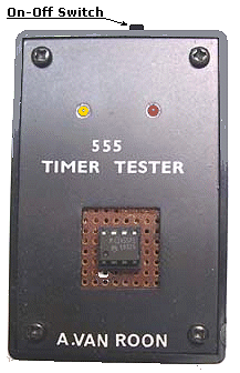
This is a Simple 555 Tester Circuit Diagram. The IC 555 is a widely used timers, control circuits, PWM, alarms, etc.. Often we set up a circuit that does not work or works differently than expected, this time the ideal is a test circuit for this IC.
This test circuit 555 is connected as an astable multivibrator when the button switch S1 is pressed, the LEDs D1 and D2 flash alternately. Ie, when the output is high D2 will light when the output is low D3 will light, and the other a Hi Lo. The speed of flashes is determined by the components R1, R2 and C1.Pressing the S1 test the 555 starts and any change in the IC flashes may consider to be defective.

Simple 50 to 300 MHz Colpitts Oscillator
Simple high efficiency Colpitts oscillator .In the higher frequency ranges, above 50 MHz, Colpitts oscillators are used because stray circuit capacitance will be in parallel with desired feedback capacitance and not cause undesirable spurious resonances that might occur with the tapped coil Hartley design.

The FM VCO shown is a grounded base design with feedback from collector to emitter. A Colpitts oscillator is one of a number of designs for electronic oscillator circuits using the combination of an inductance with a capacitor for frequency determination.As you can see in the circuit diagram , this electronic project require few electronic parts an provide a 50 MHz-300MHz VCO with a tuning range of 2:1 . link
Thursday, October 23, 2014
Simple Emergency Light
This is an automatic emergency lamp with day light sensing, means it senses darkness/night and turns ON automatically. Similarly it senses day light and turns OFF automatically. A simple emergency lamp which does not require any special equipment; even a multimeter to assemble and use. Any individual who can do a good quality soldering must be able to build this circuit successfully.
This can be easily accommodated in the defunct two 6 watt tube National Emergency Lamp or any PL tube type emergency lamp. The difference will be in the working; it will work non stop for more than 8 hours.deep discharge is taken care by the LED characteristic and over charge protection is taken care by the fixed voltage regulator.This uses a simple 3Pin fixed regulator which has a built in current limiting circuit.
Simple Emergency Light Circuit Diagram:

This can be easily accommodated in the defunct two 6 watt tube National Emergency Lamp or any PL tube type emergency lamp. The difference will be in the working; it will work non stop for more than 8 hours.deep discharge is taken care by the LED characteristic and over charge protection is taken care by the fixed voltage regulator.This uses a simple 3Pin fixed regulator which has a built in current limiting circuit.
Simple Emergency Light Circuit Diagram:

The only required adjustment is the preset which has to be set to ensure the LEDs just light up (it should be left at that position). The 5mm LDR is just mounted on top of the emergency light as shown in the photograph. LDR is used to avoid it lighting up during day time or when the room lights are ON. 2 LEDs are used in series; the dropping resistance is avoided and 2 LEDs light up with current that is required for a single LED, by which energy is saved to a great extent.
This particular circuit has been kept so simple for people who has limited access to components or in other words this is an emergency light that you can build with minimum components. In addition to circuit diagram, He has shared photographs of the prototype he made in National emergency light and a PCB design.
http://www.extremecircuits.net
Simple Radiator Temperature Iindicator
This radiator temperature indicator can be designed using electronic circuit diagram bellow .Temperature indicator consists of two special zener diode, D1 and D2, connected in series to ensure accuracy of 5.96 V Zener voltage at 25 ° C. As long as the radiator temperature not exceeding 50 ° C, thermal indicator will flash a green LED, one orange will be provided for temperatures of 50 ... 75 ° C and a red LED, for temperatures above 75 ° C.

Zener voltage will increase by 20 mV for each temperature increase of a degree Celsius temperature. Radiator temperature corresponding voltage level is compared with two reference voltages, IC1 and IC2 using. When the temperature reaches 50 ° C, IC2s output goes to logic state "1" so that T3 leads and following ignition with diode D4. At 75 ° C, IC1s output is in logic state "1" and, therefore, T2 and T3 will, so that D3 and D4 lights are off. Link
Simple Alkaline Cell Charger Circuit Diagram
This is the Simple Alkaline Cell Charger Circuit Diagram. This charger works as two channel current limited voltage source 1.6 V. Low charge current allows charging deep discharged cells (0.7 - 0.8 V) and non-rechargeable cells. Charge current can be changed by R9 and R10. With 470 Ohm is approx 7 mA. LED1 and LED indicates when cell voltage reached 1.6 V and cell is fully charged.
If power supply is disconnected, reverse discharging current is negligibly (less than 1 microA). For this feature is operational amplifier type LM324 recommended or similar type with p-n-p transistor on input. Non-rechargeable cells can be charged, but their capacity will be significantly less than rechargeable cells


Parts list
| R1 | 2,2 kohm |
| R2 | 10 kohm |
| R3 | 2,7 kohm |
| R4 | 15 kohm |
| R5, R6 | 5,6 kohm |
| R7, R8 | 22 kohm (viz text) / depend on R9, R10 (approx. 50 times greater than R9, R10) |
| R9, R10 | 470 ohm (see text) / change charge current |
| R11, R12 | 1 kohm (See text) / change LEDs current |
| R13 | 1 kohm, SMD1206 |
| C1 | 100 nF, ceramic |
| D1, D2 | 1N4148 etc. |
| T1, T2 | 2SC945 etc. |
| IC1 | TL431C |
| IC2 | LM324 |
| LED1 until LED3 | Any LED 3 mm with low power consumption / any low power 3 mm LEDs |
| Housing Articles/ cell cases AA, AAA | |
| pcb bcs67 / PCB board see fig. 2 |
Monday, October 20, 2014
Simple 300m FM Transmitter
This FM transmitter circuit is very simple and it has a acceptable transmission . The signal transited from this FM transmitter circuit can be received at almost 300 meters in open air .The circuit require a 3volts operating voltage and can be tuned anywhere in the FM band.The coil should be about 3mm in diameter and 5 turns. The wire is tinned copper wire, 0.61 mm in diameter.After the coil in soldered into place spread the coils apart about 0.5 to 1mm so that they are not touching.

If you don’t have a trim cap you can use a fixed value capacitor and you can vary the TX frequency by adjusting the spacing of the coils or placing a small piece of ferrite inside the coil , but the better way to change the transmission frequency is to use a variable capacitor .Connect a half or quarter wavelength antenna (length of wire) to the aerial point. At an FM frequency of 100 MHz these lengths are 150 cm and 75 cm respectively.
Check Inductors With This Simple Q Meter
While LCR meters are readily available at reasonable cost, they do not measure the Q of an inductor. This circuit enables you to measure the Q of inductors with the aid of an RF signal generator. A capacitor is connected in parallel with the inductor to form a tuned circuit. By varying the frequency, you can measure the resonance frequency of the tuned circuit and its -3dB bandwidth. The Q is then the resonance frequency divided by the -3dB bandwidth. Transistor Q1 is an emitter follower acting as input buffer to drive RF transformer T1. The secondary winding of T1 then drives the parallel tuned circuit formed by the inductor under test (Lx), T1’s secondary and tuning capacitor VC.
The tuned circuit so formed is buffered by JFET Q2 and transistor Q3 which form a cascode stage with about 3dB of gain. The JFET provides a high impedance so that the loading of the tuned circuit is minimal (note: an MPF102 can be substituted if you cannot obtain a 2N5485). The RF output from Q2s collector can be monitored by an oscilloscope to easily find the point of resonance and read the frequency. Alternatively, the RF output can be read by an external frequency meter. Diodes D1 & D2 and the 5.6nF capacitors form a voltage doubler rectifier to drive a 100µA DC meter so that the resonance can be found (in the absence of an oscilloscope).

Trimpot VR1 provides a sensitivity adjustment for the meter. Transformer T1 is wound on a 12mm diameter ferrite toroid core. The primary winding consists of 50 turns of 0.2mm diameter enamelled copper wire, while the secondary is a single turn consisting of a strip of brass 0.5mm thick and 2.5mm wide bent into a horseshoe shape and threaded through the centre of the toroid. VC is a small AM tuning capacitor with both gangs connected in parallel.
To measure Q, the output of the RF signal generator should be around 0.5V peak. Adjust the frequency until the meters reading peaks, then adjust VR1 so that the meter reads full scale (100µA). Read the resonance frequency F0 from the frequency scale of the signal generator or better still, the reading on a frequency meter.
Next, increase the signal frequency until the meter reads 70µA and note this frequency as F2. That done, reduce the frequency on the signal generator below the resonance frequency until the meter again reads 70µA and note this frequency as F1. The Q can now be calculated as:
Q = F0/(F2 - F1)
While using a variable tuning capacitor will enable a wider range of inductors to be tested, the main advantage is estimating the distributed capacitance of the inductor as well. To do this, you have to calibrate the tuning scale with a capacitance meter, by measuring the capacitance across the tuning capacitor with no inductor connected. This is done with the unit switched off. Marking off increments of 20pF should be sufficient.
Set the tuning capacitor to say ¼ of its maximum value and note this value as C1. Adjust the RF signal generator frequency so that the inductor under test is at resonance and note this frequency as F0. Now set the RF generator frequency to half F0, adjust the tuning capacitor until resonance and note this capacitance as C2. The distributed capacitance of the inductor is (C2 - 4C1)/3.
The tuned circuit so formed is buffered by JFET Q2 and transistor Q3 which form a cascode stage with about 3dB of gain. The JFET provides a high impedance so that the loading of the tuned circuit is minimal (note: an MPF102 can be substituted if you cannot obtain a 2N5485). The RF output from Q2s collector can be monitored by an oscilloscope to easily find the point of resonance and read the frequency. Alternatively, the RF output can be read by an external frequency meter. Diodes D1 & D2 and the 5.6nF capacitors form a voltage doubler rectifier to drive a 100µA DC meter so that the resonance can be found (in the absence of an oscilloscope).

Trimpot VR1 provides a sensitivity adjustment for the meter. Transformer T1 is wound on a 12mm diameter ferrite toroid core. The primary winding consists of 50 turns of 0.2mm diameter enamelled copper wire, while the secondary is a single turn consisting of a strip of brass 0.5mm thick and 2.5mm wide bent into a horseshoe shape and threaded through the centre of the toroid. VC is a small AM tuning capacitor with both gangs connected in parallel.
To measure Q, the output of the RF signal generator should be around 0.5V peak. Adjust the frequency until the meters reading peaks, then adjust VR1 so that the meter reads full scale (100µA). Read the resonance frequency F0 from the frequency scale of the signal generator or better still, the reading on a frequency meter.
Next, increase the signal frequency until the meter reads 70µA and note this frequency as F2. That done, reduce the frequency on the signal generator below the resonance frequency until the meter again reads 70µA and note this frequency as F1. The Q can now be calculated as:
Q = F0/(F2 - F1)
While using a variable tuning capacitor will enable a wider range of inductors to be tested, the main advantage is estimating the distributed capacitance of the inductor as well. To do this, you have to calibrate the tuning scale with a capacitance meter, by measuring the capacitance across the tuning capacitor with no inductor connected. This is done with the unit switched off. Marking off increments of 20pF should be sufficient.
Set the tuning capacitor to say ¼ of its maximum value and note this value as C1. Adjust the RF signal generator frequency so that the inductor under test is at resonance and note this frequency as F0. Now set the RF generator frequency to half F0, adjust the tuning capacitor until resonance and note this capacitance as C2. The distributed capacitance of the inductor is (C2 - 4C1)/3.
Simple Function Generator Circuit Diagram using NE566
Simple circuit function generator that generates square wave and triangular or sawtooth. The frequency is determined by R and C1. For the sawtooth wave output is on pin 4 and the voltage of 6 V, while for the square wave output is on pin 3. The function generator circuit uses only one 566 and can be connected to output amplified audio. The frequency is set by potentiometer R2.
Function generator circuit using NE566 Circuit Diagram

Simple Timer with Transistor Circuit Diagram
The below Simple Timer with Transistor Circuit Diagram is a simple timer that uses only two Darlington transistors and a capacitor base to generate a delay. When SW1 is pressed, the timer starts, the time setting is set by VR1. The duration of the timer is given by the values of the potentiometer VR1 and the capacitor C1 that this circuit is 220 pF. To reach other durations of time must change the values of these two components.
Timer with Transistor Circuit Diagram

Simple Bells Ring Generator Circuit Schematic
This circuit generates a dual-tone bells ringing similar to most door-bell units. It can be used in many applications other than door-bell. In the Notes below several options will be given in order to suit different needs. The circuit as shown in the diagram generates a "Ding-tone" when P1 is pressed and a "Dong-tone" when P1 is released. IC1D is the first-tone frequency generator and IC1F generates the second-tone.
Q2, Q5 and related components act as shape and decay controls of the two tones, trying to imitate as close as possible the bells sound. Their outputs are mixed (R7 & R13), filtered (C5) and boosted by a simple class-A audio amplifier (Q3 & Q4) in order to drive the loudspeaker. The amplifier is switched-on by Q1 when P1 is pressed, then is switched-off some seconds after P1 is released: this time-delay is fixed by C1 & R2. In this way the circuit will draw a negligible current when in stand-by mode.
Circuit diagram:
Q2, Q5 and related components act as shape and decay controls of the two tones, trying to imitate as close as possible the bells sound. Their outputs are mixed (R7 & R13), filtered (C5) and boosted by a simple class-A audio amplifier (Q3 & Q4) in order to drive the loudspeaker. The amplifier is switched-on by Q1 when P1 is pressed, then is switched-off some seconds after P1 is released: this time-delay is fixed by C1 & R2. In this way the circuit will draw a negligible current when in stand-by mode.
Circuit diagram:

Bells Ring Generator Schematic Circuit Diagram
Parts:
R1,R3,R7,R9,R13_10K 1/4W Resistors
R2_______________1M5 1/4W Resistor
R4______________27K 1/4W Resistor
R5,R11__________47K 1/4W Resistors
R6,R12_________220K 1/4W Resistors
R8_______________2M2 1/4W Resistor
R10_____________33K 1/4W Resistor
C1_______________2µ2 25V Electrolytic Capacitor
C2______________47µF 25V Electrolytic Capacitor
C3,C8___________10µF 25V Electrolytic Capacitors
C4,C7___________10nF 63V Polyester Capacitors
C5,C6__________100nF 63V Polyester Capacitors
C9_______________4µ7 25V Electrolytic Capacitor
C10______________1µF 25V Electrolytic Capacitor
D1-D5_________1N4148 75V 150mA Diodes
IC1__________MC14106 or 40106 Hex Schmitt Inverter IC
Q1_____________BC337 45V 800mA NPN Transistor
Q2,Q3,Q5_______BC238 25V 100mA NPN Transistors
Q4 ____________BC327 45V 800mA PNP Transistor
PH______________Photo resistor (any type) (see Notes)
P1______________SPST Pushbutton (see Notes)
SW1_____________SPST Switch
SPKR____________8 Ohm Loudspeaker
B1______________3V Battery (two 1.5V AA or AAA cells in series etc.)
Parts added to optional modification:
R14____________220K 1/4W Resistor
R15______________1M 1/4W Resistor
Notes:
- To obtain a "Ding-Dong" operation when pushing on P1, no matter when it is released, you must modify the circuit as shown in the frame placed at the low-right corner of the circuit diagram. D4 must be removed. C10 & R15 set the time-delay separating first and second tone.
- To obtain a one-tone-only generator, wire the circuit as in the optional modification, making the following changes:
- C9 = 100nF 63V Polyester Capacitor.
- Omit R9 to R13 & R15; C7, C8 & C10; D2, D4, D5 & Q5.
- Connect to negative supply pins 11 & 13 of IC1 and left open pins 10 & 12.
- An amusing application of this circuit wired as in the original schematic, is to use a photo-resistor in place of P1, then placing the unit near the flashing lamps of your Christmas tree. A soft bell sound may be heard at switch-on and switch-off of the lamp chosen.
- To obtain higher output power you may substitute R8, Q3 & Q4 with an audio amplifier IC like the LM386 or LM380. In this case power supply must be raised to 6 - 12V but at the same time R4 & R10 should be changed to adjust bell-tone frequencies.
- Good tone frequencies are roughly 2000 and 1650Hz respectively.
- When in stand-by mode, current drawing of the circuit is 200µA @ 3V supply: therefore SW1 can be omitted.
Source: Red Free Circuit Models
Simple 50V Bench Power Supply
An 50v bench power supply can be made using electronic diagram below which is designed using LM10 op amp and 2n3055 transistors. This LM10 2n3055 50v bench power supply allows an output voltage regulation in a range between 0 and 50 volts and the output current can be limited to a maximum of 2A. Output voltage increases linearly with the amount of resistance potentiometer P1, while the current can be adjusted linear using potentiometer P3. Potentiometer P2 serves to regulate maximum output current (maximum value is 2A).
Simple Alarm Residential 5 sectors Circuit Diagram
This is a circuit of an alarm residential sectors 5, or 5 areas that are monitored separately, it also has a panic button, timing system, is powered by the network jointly by battery v. 12. It is very simple and uses only three integrated circuits and transistors.
Simple Alarm Residential 5 sectors Circuit Diagram

Simple 1000W Power Inverter circuit diagram
This is the power inverter circuit based MOSFET RFP50N06. The inverter capable to handle loads up to 1000W, it’s depended on your power inverter transformer. The RFP50N06 Fets are rated at 50 Amps and 60 Volts. Heatsink is required for cooling the MOSFETs. You may add some MOSFETs with parallel connection to get more power. It is recommended to have a “Fuse” in the Power Line and to always have a “Load connected”, while power is being applied.
Simple 1000W Power Inverter circuit diagram

Thursday, October 16, 2014
Simple UPS Power Supply
This circuit is a simple form of the commercial UPS, the circuit provides a constant regulated 5 Volt output and an unregulated 12 Volt supply. In the event of electrical supply line failure the battery takes over, with no spikes on the regulated supply.

This circuit can be adapted for other regulated and unregulated voltages by using different regulators and batteries. For a 15 Volt regulated supply use two 12 Volt batteries in series and a 7815 regulator. There is a lot of flexibility in this circuit.
TR1 has a primary matched to the local electrical supply which is 240 Volts in the UK. The secondary winding should be rated at least 12 Volts at 2 amp, but can be higher, for example 15 Volts. FS1 is a slow blow type and protects against short circuits on the output, or indeed a faulty cell in a rechargeable battery. LED 1 will light ONLY when the electricity supply is present, with a power failure the LED will go out and output voltage is maintained by the battery. The circuit below simulates a working circuit with mains power applied:
Between terminals VP1 and VP3 the nominal unregulated supply is available and a 5 Volt regulated supply between VP1 and VP2. Resistor R1 and D1 are the charging path for battery B1. D1 and D3 prevent LED1 being illuminated under power fail conditions. The battery is designed to be trickle charged, charging current defined as :-
(VP5 - 0.6 ) / R1
where VP5 is the unregulated DC power supply voltage.
D2 must be included in the circuit, without D2 the battery would charge from the full supply voltage without current limit, which would cause damage and overheating of some rechargeable batteries. An electrical power outage is simulated below:
Note that in all cases the 5 Volt regulated supply is maintained constantly, whilst the unregulated supply will vary a few volts.
Standby Capacity
The ability to maintain the regulated supply with no electrical supply depends on the load taken from the UPS and also the Ampere hour capacity of the battery. If you were using a 7A/h 12 Volt battery and load from the 5 Volt regulator was 0.5 Amp (and no load from the unregulated supply) then the regulated supply would be maintained for around 14 hours. Greater A/h capacity batteries would provide a longer standby time, and vice versa.
Simple Sleeping Aid Schematic Circuit Diagram
Many people experienced sleeping well in natural surroundings, into a tent or a wooden hut. This fact is due not only to the healthy atmosphere but also from our unconscious ability to perceive natural Earths magnetic-fields. The circuit generates this type of Geo-magnetic-fields and lets us perceive them: in this manner our brain is surrounded by an ideal environment for a sound sleep. (N.B. Basic ideas for this circuit are coming from German papers).
Circuit operation:
IC2C and IC2D generate two square waves at about 1.2 and 5 Hz respectively. These wave-forms are converted into 60µS pulses at the same frequencies by means of C5 & C6 and mixed at Q1 Base. This transistor drives the Radiator coil with a scalar series of pulses of 60µS length and 9V amplitude. IC1, IC2A & IC2B form the timer section.
C1 & R2 provide auto-reset of IC1 at switch-on. The internal oscillator of IC1 drives the 14 stage ripple counter and, after about 15 minutes, output pin 1 goes high. Pin 3 of IC2A goes low and stops IC2C & IC2D oscillation. If SW2 is left open (Alternate mode operation), after 15 minutes pin 1 of IC1 goes low, pin 3 of IC2A goes high and oscillators are enabled again.
If SW2 is closed (Stop mode operation), the first time output pin 1 of IC1 goes high, the internal oscillator of the IC is disabled by means of D1. Therefore the circuit remains off until a reset pulse is applied to pin 12 by means of P1 or when the whole device is switched-off and then restarted. The same thing occurs when SW1 is switched on 30 or 60 minutes positions, obviously changing time length.
IC2B drives pilot LED D2 which operates in the following three modes:
IC2C and IC2D generate two square waves at about 1.2 and 5 Hz respectively. These wave-forms are converted into 60µS pulses at the same frequencies by means of C5 & C6 and mixed at Q1 Base. This transistor drives the Radiator coil with a scalar series of pulses of 60µS length and 9V amplitude. IC1, IC2A & IC2B form the timer section.
C1 & R2 provide auto-reset of IC1 at switch-on. The internal oscillator of IC1 drives the 14 stage ripple counter and, after about 15 minutes, output pin 1 goes high. Pin 3 of IC2A goes low and stops IC2C & IC2D oscillation. If SW2 is left open (Alternate mode operation), after 15 minutes pin 1 of IC1 goes low, pin 3 of IC2A goes high and oscillators are enabled again.
If SW2 is closed (Stop mode operation), the first time output pin 1 of IC1 goes high, the internal oscillator of the IC is disabled by means of D1. Therefore the circuit remains off until a reset pulse is applied to pin 12 by means of P1 or when the whole device is switched-off and then restarted. The same thing occurs when SW1 is switched on 30 or 60 minutes positions, obviously changing time length.
IC2B drives pilot LED D2 which operates in the following three modes:
- flashes quickly and almost randomly when the Radiator coil is driven
- flashes somewhat slowly and regularly when the Radiator coil is pausing during the Alternate mode operation
- is off when the circuit auto-stops (Stop mode operation)
Circuit diagram:

Sleeping Aid Circuit Diagram
Parts:
R1 = 1K 1/4W Resistors
R2 = 10K 1/4W Resistor
R3 = 10M 1/4W Resistors
R4 = 2M2 1/4W Resistors
R5 = 1K 1/4W Resistors
R6 = 10M 1/4W Resistors
R7 = 2M2 1/4W Resistors
R8 = 4K7 1/4W Resistors
R9 = 4K7 1/4W Resistors
C1 = 47µF 25V Electrolytic Capacitors
C2 = 100nF 63V Polyester Capacitor
C3 = 330nF 63V Polyester Capacitors
C4 = 330nF 63V Polyester Capacitors
C5 = 15nF 63V Polyester Capacitors
C6 = 15nF 63V Polyester Capacitors
C7 = 47µF 25V Electrolytic Capacitors
D1 = 1N4148 75V 150mA Diodes
D2 = LED (any type) (see Notes)
D3 = 1N4148 75V 150mA Diodes
D4 = 1N4148 75V 150mA Diodes
D5 = 1N4148 75V 150mA Diodes
IC1 = 4060 14 stage ripple counter and oscillator IC
IC2 = 4093 Quad 2 input Schmitt NAND Gate IC
Q1 = BC327 45V 800mA PNP Transistor
L1 = Radiator coil (see Notes)
P1 = SPST Pushbutton
SW1 = 2 poles 4 ways rotary switch
SW2 = SPST Slider Switch
B1 = 9V PP3 Battery, Clip for PP3 Battery
Features:
R1 = 1K 1/4W Resistors
R2 = 10K 1/4W Resistor
R3 = 10M 1/4W Resistors
R4 = 2M2 1/4W Resistors
R5 = 1K 1/4W Resistors
R6 = 10M 1/4W Resistors
R7 = 2M2 1/4W Resistors
R8 = 4K7 1/4W Resistors
R9 = 4K7 1/4W Resistors
C1 = 47µF 25V Electrolytic Capacitors
C2 = 100nF 63V Polyester Capacitor
C3 = 330nF 63V Polyester Capacitors
C4 = 330nF 63V Polyester Capacitors
C5 = 15nF 63V Polyester Capacitors
C6 = 15nF 63V Polyester Capacitors
C7 = 47µF 25V Electrolytic Capacitors
D1 = 1N4148 75V 150mA Diodes
D2 = LED (any type) (see Notes)
D3 = 1N4148 75V 150mA Diodes
D4 = 1N4148 75V 150mA Diodes
D5 = 1N4148 75V 150mA Diodes
IC1 = 4060 14 stage ripple counter and oscillator IC
IC2 = 4093 Quad 2 input Schmitt NAND Gate IC
Q1 = BC327 45V 800mA PNP Transistor
L1 = Radiator coil (see Notes)
P1 = SPST Pushbutton
SW1 = 2 poles 4 ways rotary switch
SW2 = SPST Slider Switch
B1 = 9V PP3 Battery, Clip for PP3 Battery
Features:
- Generates a natural electromagnetic-field
- Makes easier to fall asleep
- Induces a prolonged and sound sleep without drugs
- No side effects
Use of this circuit:
- Select a timing option by means of the rotary switch SW1.
- Choose 15, 30 or 60 minutes operation.
- Select "Stop" or "Alternate" mode operation by means of SW2.
- With SW2 closed (Stop mode operation) the electromagnetic radiation stops after the pre-set time is elapsed.
- With SW2 opened (Alternate mode operation) the device operates for the pre-set time, then pauses for the same amount of time: this cycle repeats indefinitely.
- Place the unit under the pillow and sleep like a log.
- To reset a cycle press P1 pushbutton.
Notes:
- L1 is obtained by winding randomly 600 turns of 0.2 mm. enameled wire on a 6 mm. diameter, 40 mm. long, steel bolt. Secure the winding with insulating tape.
- Mean current drawing is about 7mA, decreasing to less than 4mA during pauses when in Alternate mode operation.
- Battery life can be dramatically increased omitting LED D2 and its associated resistor R5.
- Use a plastic box to enclose the circuit: metal cases can severely limit electromagnetic radiation.
Friday, September 26, 2014
Simple 2 Watt Small Switching Power Supply Circuit Diagram
In this small switching power supply, a Schmitt trigger oscillator is used to drive a switching transistor that supplies current to a small inductor. Energy is stored in the inductor while the transistor is on, and released into the load circuit when the transistor switches off.
2 Watt Small Switching Power Supply Circuit Diagram

The output voltage is dependent on the load resistance and is limited by a zener diode that stops the oscillator when the voltage reaches about 14 volts. Higher or lower voltages can be obtained by adjusting the voltage divider that feeds the zener diode. The efficiency is about 80% using a high Q inductor.
Simple Automatic Switch For Audio Power Amplifier
Simple Automatic Switch For Audio Power Amplifier.Circuit of an automatic switch for audio power amplifier stage is presented here. The circuit uses stereo preamplifier output to detect the presence of audio to switch the audio power amplifier on only when audio is present. The circuit thus helps curtail power wastage. IC1 is used as an inverting adder. The input signals from left and right channels are combined to form a common signal for IC2, which is used as an open loop comparator. IC3 (NE556) is a dual timer. Its second section, i.e., IC3(b), is configured as monostable multivibrator. Output of IC3(b) is used to switch the power amplifier on or off through a Darlington pair formed by transistors T1 and T2. IC3(a) is used to trigger the monostable multivibrator whenever an input signal is sensed.
Circuit diagram:
Automatic Switch For Audio Power Amplifier Circuit Diagram
Under ‘no signal’ condition, pin 3 of IC2 is negative with respect to its pin 2. Hence the output of IC2 is low and as a result output of IC3(a) is high. Since there is no trigger at pin 8 of IC3(b), the output of IC3(b) will be low and the amplifier will be off. When an input singal is applied to IC1, IC2 converts the inverted sum of the input signals into a rectangular waveform by comparing it with a constant voltage which can be controlled by varying potentiometer VR1. When the output of IC2 is high, output pin 5 of IC3 goes low, thus triggering the monostable multivibrator. As soon as the audio input to IC1 stops, pin 5 of IC3 goes high and pin 1 of IC3 discharges through capacitor C3, thus resetting the monostable multivibrator.
Hence, as long as input signals are applied, the amplifier remains ‘on.’ When the input signals are removed, i.e., when signal level is zero, the amplifier switches off after the mono flip-flop delay period determined by the values of resistor R8 and capacitor C3. If no input signals are sensed within this time, the amplifier turns off—else it remains on. Power supply for the circuit can be obtained from the power supply of the amplifier. Hence, the circuit can be permanently fitted in the amplifier box itself. The main switch of the amplifier should be always kept on. Resistors R1 and R2 are used to divide single voltage supply into two equal parts.
Capacitors C1 and C2 are used as regulators and also as an AC bypass for input signals. Diode D1 is used so that loading fluctuations in power amplifier do not affect circuit regulation. Transisitor T2 acts as a high voltage switch which may be replaced by any other high voltage switching transistor satisfying amplifier current requirements. Value of resistor R10 should be modified for large current requirement. The LED glows when the amplifier is on. The circuit is very useful and relieves one from putting the amplifier on and off every time one plays a cassette or radio etc.
Subscribe to:
Posts (Atom)