Showing posts with label with. Show all posts

Friday, October 24, 2014

Low drop Regulator with Indicator Circuit Diagram

Even today much logic is still powered from 5 volts and it then seems obvious to power the circuit using a standard regulator from a rectangular 9-V battery. A disadvantage of this approach is that the capacity of a 9-V battery is rather low and the price is rather high. Even the NiMH revolution, which has resulted in considerably higher capacities of (pen-light) batteries, seems to have escaped the 9-V battery generation. It would be cheaper if 5 volts could be derived from 6 volts, for example. That would be 4 ‘normal’ cells or 5 NiMH- cells. Also the ‘old fashioned’ sealed lead- acid battery would be appropriate, or two lithium cells.
 
Circuit diagram : 
Low-drop Regulator with Indicator-Circuit-Diagram
Low-drop Regulator with Indicator Circuit Diagram
 
Using an LP2951, such a power supply is easily realised. The LP2951 is an ever- green from National Semiconductor, which you will have encountered in numerous  Elektor Electronics designs already. This IC can deliver a maximum current of 100 mA at an input voltage of greater than 5.4 V. In addition to this particular version, there are also versions available for 3.3 and 3 V output, as well as an adjustable version.  In this design we have added a battery indicator, which also protects the battery from too deep a discharge. As soon as the IC has a problem with too low an input voltage, the ERROR output will go low and the regulator is turned off via IC2d, until a manual restart is provided with the RESET pushbutton.
 
The battery voltage is divided with a few resistors and compared with the reference voltage (1.23 V) of the regulator IC. To adapt the indicator for different voltages you only need to change the 100-k resistor. The comparator is an LP339. This is an energy-friendly version of the LM339. The LP339 consumes only 60 µA and can sink 30 mA at its output. You can also use the LM339, if you happen to have one around, but the current consumption in that case is 14 times higher (which, for that matter, is still less than 1 mA).
 
Finally, the LP2951 in the idle state, consumes about 100 µA and depend- ing on the output current to be deliv- ered, a little more. 


Read More..

Thursday, October 23, 2014

10 000x With One Transistor

For a collector follower with emitter resistor, you’ll often find that the gain per stage is no more than 10 to 50 times. The gain increases when the emitter resistor is omitted. Unfortunately, the distortion also increases. With a ubiquitous transistor such as the BC547B, the gain of the transistor is roughly equal to 40 times the collector current (Ic), provided the collector current is less than a few milliamps. This value is in theory equal to the expression q/KT, where q is the charge of the electron, K is Boltzmann’s constant and T is the temperature in Kelvin.

For simplicity, and assuming room temperature, we round this value to 40. For a single stage amplifier circuit with grounded emitter it holds that the gain Uout /Uin (for AC voltage) is in theory equal to SRc. As we observed before, the slope S is about 40Ic. From this follows that the gain is approximately equal to 40I cRc. What does this mean? In the first instance this leads to a very practical rule of thumb: that gain of a grounded emitter circuit amounts to 40·I c·Rc, which is equal to 40 times the voltage across the collector resistor.

If Ub is, for example, equal to 12 V and the collector is set to 5V, then we know, irrespective of the values of the resistors that the gain will be about 40R(12–5) = 280. Notable is the fact that in this way the gain can be very high in theory, by selecting a high power supply voltage. Such a voltage could be obtained from an isolating transformer from the mains. An isolating transformer can be made by connecting the secondaries of two transformers together, which results in a galvanically isolated mains voltage.

Circuit diagram:
10,000x With One Transistor Circuit diagram

That means, that with a mains voltage of 240 Veff there will be about 340 V DC after rectification and filtering. If in the amplifier circuit the power supply voltage is now 340 V and the collector voltage is 2 V, then the gain is in theory equal to 40 x (340–2). This is more than 13,500 times! However, there are a few drawbacks in practice. This is related to the output characteristic of the transistor. In practice, it turns out that the transistor does actually have an output resistor between collector and emitter.

This output resistance exists as a transistor parameter and is called ‘hoe’. In normal designs this parameter is of no consequence because it has no noticeable effect if the collector resistor is not large. When powering the amplifier from 340 V and setting the collector current to 1 mA, the collector resistor will have a value of 338 k. Whether the ‘hoe’-parameter has any influence depends in the type of transistor. We also note that with such high gains, the base-collector capacitance in particular will start to play a role.

As a consequence the input frequency may not be too high. For a higher bandwidth we will have to use a transistor with small Cbc, such as a BF494 or perhaps even an SHF transistor such as a BFR91A. We will have to adjust the value of the base resistor to the new hfe. The author has carried out measurements with a BC547B at a power supply voltage of 30 V. A value of 2 V was chosen for the collector voltage. Measurements confirm the rule of thumb. The gain was more than 1,000 times and the effects of ‘hoe’ and the base-collector capacitance were not noticeable because of the now much smaller collector resistor.
 
 
Author: Gert Baars
Read More..

Monday, October 20, 2014

Check Inductors With This Simple Q Meter


While LCR meters are readily available at reasonable cost, they do not measure the Q of an inductor. This circuit enables you to measure the Q of inductors with the aid of an RF signal generator. A capacitor is connected in parallel with the inductor to form a tuned circuit. By varying the frequency, you can measure the resonance frequency of the tuned circuit and its -3dB bandwidth. The Q is then the resonance frequency divided by the -3dB bandwidth. Transistor Q1 is an emitter follower acting as input buffer to drive RF transformer T1. The secondary winding of T1 then drives the parallel tuned circuit formed by the inductor under test (Lx), T1’s secondary and tuning capacitor VC.

The tuned circuit so formed is buffered by JFET Q2 and transistor Q3 which form a cascode stage with about 3dB of gain. The JFET provides a high impedance so that the loading of the tuned circuit is minimal (note: an MPF102 can be substituted if you cannot obtain a 2N5485). The RF output from Q2s collector can be monitored by an oscilloscope to easily find the point of resonance and read the frequency. Alternatively, the RF output can be read by an external frequency meter. Diodes D1 & D2 and the 5.6nF capacitors form a voltage doubler rectifier to drive a 100µA DC meter so that the resonance can be found (in the absence of an oscilloscope).

Check inductors with this simple Q meter
Trimpot VR1 provides a sensitivity adjustment for the meter. Transformer T1 is wound on a 12mm diameter ferrite toroid core. The primary winding consists of 50 turns of 0.2mm diameter enamelled copper wire, while the secondary is a single turn consisting of a strip of brass 0.5mm thick and 2.5mm wide bent into a horseshoe shape and threaded through the centre of the toroid. VC is a small AM tuning capacitor with both gangs connected in parallel.

To measure Q, the output of the RF signal generator should be around 0.5V peak. Adjust the frequency until the meters reading peaks, then adjust VR1 so that the meter reads full scale (100µA). Read the resonance frequency F0 from the frequency scale of the signal generator or better still, the reading on a frequency meter.

Next, increase the signal frequency until the meter reads 70µA and note this frequency as F2. That done, reduce the frequency on the signal generator below the resonance frequency until the meter again reads 70µA and note this frequency as F1. The Q can now be calculated as:

Q = F0/(F2 - F1)

While using a variable tuning capacitor will enable a wider range of inductors to be tested, the main advantage is estimating the distributed capacitance of the inductor as well. To do this, you have to calibrate the tuning scale with a capacitance meter, by measuring the capacitance across the tuning capacitor with no inductor connected. This is done with the unit switched off. Marking off increments of 20pF should be sufficient.

Set the tuning capacitor to say ¼ of its maximum value and note this value as C1. Adjust the RF signal generator frequency so that the inductor under test is at resonance and note this frequency as F0. Now set the RF generator frequency to half F0, adjust the tuning capacitor until resonance and note this capacitance as C2. The distributed capacitance of the inductor is (C2 - 4C1)/3.
Read More..

Stereo Preamplifier With Bass Boost

High Quality, simple design, DC 20v to 30v supply
This preamplifier was designed to cope with CD players, tuners, tape recorders etc., providing an ac voltage gain of 4, in order to drive less sensitive power amplifiers. As modern Hi-Fi home equipment is frequently fitted with small loudspeaker cabinets, the bass frequency range is rather sacrificed. This circuit features also a bass-boost, in order to overcome this problem. You can use a variable resistor to set the bass-boost from 0 to a maximum of +16dB @ 30Hz. If a fixed, maximum boost value is needed, the variable resistor can be omitted and substituted by a switch.
Circuit Diagram:
stereoPreamplierWithBass-boost Stereo Preamplifier With Bass Boost Circuit Diagram

Parts:
P1 = 10K
P2 = 100K
R1 = 100K
R2 = 100K
R3 = 15K
R4 = 10K
R5 = 22K
R6 = 15K
R7 = 1K
R8 = 470R
C1 = 2.2uF-25v
C2 = 2.2uF-25v
C3 = 470uF-35v
C4 = 1uF-35V
C5 = 2.2uF-25v
C6 = 47nF-63v
C7 = 22uF-25v
IC1 = TL072, Opamp
SW1 = DPST Switch
Notes:
  • Schematic shows left channel only, but R1, R2, R3 and C1, C2, C3 are common to both channels.
  • For stereo operation P1, P2 (or SW1), R4, R5, R6, R7, R8 and C4, C5, C6, C7 must be doubled.
  • Numbers in parentheses show IC1 right channel pin connections.
  • A log type for P2 ensures a more linear regulation of bass-boost.
  • Needing a simple boost-in boost-out operation, P2 must be omitted and SW1 added as shown in the diagram.
  • For stereo operation SW1 must be a DPST type.
  • Please note that, using SW1, the boost is on when the switch is open, and off when the switch is closed.

Read More..

Simple Timer with Transistor Circuit Diagram

The below Simple Timer with Transistor Circuit Diagram is a simple timer that uses only two Darlington transistors and a capacitor base to generate a delay. When SW1 is pressed, the timer starts, the time setting is set by VR1. The duration of the timer is given by the values ​​of the potentiometer VR1 and the capacitor C1 that this circuit is 220 pF. To reach other durations of time must change the values ​​of these two components.

Timer with Transistor Circuit Diagram

Simple Timer with Transistor Circuit Diagram

Read More..

How to Build Timer with Musical Alarm

The timer with Musical Alarm  use famous CMOS oscillator/divider IC (IC1 ). Although this circuit operates in 9V its standby current drain is very low. The time delay of timer circuit can be adjusted by adjusting the preset VR1. The base of npn transistor T1 is connected to pin 3 of IC1 through resistor R4 and its emitter terminal is connected with pin 2 of melody generator IC­ (IC2) in order to provide positive supply when adjusted time delay is over.

Timer with Musical Alarm Circuit Diagram

Here the zener diode ZD1 is used as regulator which reduce power supply to required for operation of IC2 i.e. 3.3V. Lastly for music output the output from pin 1 of IC2 is fed to loud speaker via driver transistor and its volume is controlled by preset VR2. For starting the timer power is supplied by pressing switch SW1. Link


Parts list

Resistor (all ¼-watt, ±5%)
R1 = 1.2 MΩ
R2 = 2.2 MΩ
R3 = 56 KΩ
R4, R5, R6 = 1 KΩ
VR1 = 1 MΩ
VR2 = 1 KΩ

Capacitors
C1 = 0.01 µF
C2 = 0.22 µF
C3 = 1 µF/25V

Semiconductors
IC1 = CD4060 (CMOS oscillator /divider IC)
IC2 = UM66 (melody generator)
T1, T2 = BC547

Miscellaneous
SW1 = on/off switch
9V battery
LS1 = 8Ω, 0.5W speaker

If You Enjoyed This Project My Pleasure Take 5 Seconds To Share It.
Read More..

Thursday, February 27, 2014

Power Supply with High Voltage Isolation

Occasionally you come across some unusual  situations when setting up measurement  systems. The author once had to set up a system to register the vibrations and strain supposed to be  present in a contactor that operated at a voltage of 25 kVAC.
One of the biggest problems with this project turned out to be the power supply for  the measurement system. Since it required  a power of about 30 W it wasn’t possible to  use batteries since the system had to operate  for many hours at a time. A logical solution  would seem to be to use an isolating trans-former, but still.25 kVAC means a peak volt-age approaching 40 kV, and on top of that  you would have to include a safety margin. In  addition, everything that is connected to high  voltage lines should also be able to withstand  lighting strikes!
Circuit diagram :
Power Supply with High Voltage Isolation-Circuit Diagram
Power Supply with High Voltage Isolation Circuit Diagram
Consequently the isolation should be able to  cope with a test voltage of 150 kV, which is a  lot to ask of the isolating material.
After extensive research no supplier could be  found for a transformer rated at 50 W, 230 V  primary, 12 V secondary and an isolation of  25 kVAC. Because of this, a dynamic system  had to be used that unfortunately suffers a  bit from wear and tear. This system consists  of a 50 W 3-phase motor connected up via an  isolating drive-shaft to a 30 W generator (a  3-phase servo motor that was used as a generator), which provides the power for the data  logger and associated electronics.
Because a 3-phase generator was used, the  voltage obtained after full-wave rectification (via D1 and D4 to D8) already looked good,  also because the revs of the generator was  fairly high. The secondary supply can there-fore remain fairly simple. The main supply of 9 VDC is stabilised by IC3, an LM317T. From  there it is fed to a few small DC/DC modules  (IC1, IC4, IC5), which supply voltages of +5 V,  +30 V and -9 V, which are required by the other parts of the circuit. IC2 (LM566, a volt-age controlled oscillator) makes LED D2 flash  when the supply voltage is present.pply-with-high-voltage.html
Read More..

Wednesday, February 5, 2014

Schematic Audio Power Amplifier with IC AN7105

This Schematic Circuit Audio Amplifier use IC AN7105 , minimum voltage 1,5 volt and maximum voltage 9,5 volt. This is a low voltage Amplifier , with output speaker stereo 2 X 0,38 watt . Its so low power amplifier. Impedance speaker is 32 Ohm ,with Frequency 20 Hz -20 kHz.

See this Circuit and package IC AN7105 below :


Package IC is DIP-18

Click to view Enlarge


Read More..

Sunday, February 2, 2014

Toggle switch with Infra Red IR

Toggle switch in this article is a series of toggle switches that are controlled by infrared light. The series toggle switch is made from a combination of data flip-flop CD4013 2 units.
Receiver circuit of the infrared light signals arranged with infrared receiver as found on television remote receiver. Infrared signal from remote is used as clock signals and data to the data flip-flop first. then the second flip-flop data set as a toggle flip-flop toggle the output signal is used to drive the relay. for more details can be seen in thethe following image .


Toggle switch with Infra Red IR


Series Toggle Switch With Infra Red (IR) that is required to supply voltage range of 12VDC and the output of Toggle Switch With Infra Red (IR) is dapt used to turn on the lights or other electronic devices with DC or AC voltage source. Series Toggle Switch With Infra Red (IR) was isolated from the load that is placed for use as the final relay.
Read More..

Monday, January 27, 2014

Simple Amplifier with C945 MJE340 and TIP3055

This simple amplifier does sound good quality Power output about 10 - 14 Watts with Supply voltage about 34 - 36 Volt DC. It requires a preamp in the function of it hasnt got much advance. It requires cumbersome heat up sinks and a great transformer and a enormous power supply and alert wiring, but taking part in the bottom it is enormously regular and it sounds very good. The zener diode rubbish every wave future from the power supply, But you still barely aspire a ripple of 10mV be very successful. The swell triumph the input is enlarged, so the zener diode gets free of with the intention of, but whatever swell in attendance is wish still catch the power stage. The Buffer Stage using transistor C945 , Driver Stage Using MJE340 and Booster Stage using TIP3055 . The Transistor are using NPN transitor.

Simple Amplifier using with MJE340 TIP3055 Circuit
Simple Amplifier using with MJE340 TIP3055 Schematic Circuit Diagram
Read More..

Sunday, January 26, 2014

12 Volt Charger Circuit with LM350

The strength supply routine structure is developed as a resource of continuous present with adverse heat range coefficient. Transistor Q1 (BD 140) is used as a heat range indicator. transistor Q2 is used to avoid the strength supply from discharging through R1 when strength is out of stock. Getting routine is developed depending on the LM350 present regulator IC. The result present of the battery charger can be altered between 13-15 V by various the POT R6.


LM350 will try to keep the present decrease between the feedback pin and result pin at a continuous value of 1.25V. So there will be a continuous present circulation through resistor R1. Q1 act here as a heat range indicator with the help of R6/R3/R4 elements that are more or less manages the platform present of Q1. As relationship emitter / platform of transistor Q1, the same as other semiconductors, containing the heat range coefficient of-2mV / ° C, the present result will also display a bad heat range coefficient. This one is just a aspect of 4 huge, because the difference of the emitter / platform of Q1 is increased by a aspect of category P1/R3/R4. This causes some-8mV / ° C. LED will lighting whenever strength is available.
Read More..

Monday, January 20, 2014

700W Power Amplifier with 2SC5200 2SA1943

700W Amplifier Adjust the amplifier power 700W looks calm, but we requirement not put out of your mind to the adjustment happening forcing transistors, the whole relating to-engagement of frequency offset. It is compulsory to change the current insurance rule which serves to guard the final transistors. Their tendency to happen allowable to keep the transistors in the SOAR characteristics. primary it was needed to evaluate all the necessary resistors and subsequently measured to verify the accuracy of the calculations, it is managed with satisfactory results. Peripheral changes required in support of it to be there able to consistently amplifier to supply power. - First you need to restore the 2k2 resistors stylish string with the LEDs on Zenerovými resistors with upper wattage. be enough 1/2W resistors, power loss next to 80V +-based 1W. - therefore was traded 1k2 resistor in the pointer resistor by the side of 620 ohms. 

700W Power Amplifier with 2SC5200, 2SA1943
700W Power Amplifier with 2SC5200, 2SA1943 Circuit Diagram
Which is the initial reap has doubled, so at this point is the overall gain amplifier 40 and the limit excitation is sufficient to 1V rms. - Předbudiči transistors were replaced by stronger MJE15032/33 since KF467/470 are permitted satellite dish current 20mA - by the side of the exciter output stages are used the same transistors for example the output stage. - add up to of terminals of transistors has been increased to eight pairs - It had to occur to compensate designed for the excitation level by calculation a capacitor 10pF to 47pF + 22K appendage. This led to a slight "gradual" amplifiers, but this did not affect the ensuing parameters. This power is tuned correctly in support of this type of terminal transistors 2SA1943/2SC5200. 

With with the purpose of it is a least assessment next to which the amplifier operates stably exclusive of pass by the side of the rising and falling edges of the genuine. - The ultimate adjustment, the adjustment terminal current protection transistor. The SOAR transistor characteristics shows with the intention of the most allowable radio dish current once the voltage of 1.5 A is ideal in favor of cooling, so its essentially not as much of. Therefore, the current protection is customary to 12A, single-arm. This impersonate protection SOAR transistor characteristics. curt-circuit current is regarding 6 A which is about 075A for every transistor. This is far beneath the SOAR characteristics. The mechanical design is relatively clear-cut, the transistors are placed on the two cooling profiles with a height of 66 mm, width 44mm, overall part 260mm. They are twisted contrary to each one other in this way, from the cooling tunnel. Coolers are attaching the nylon aid which allows the compilation of transistors exclusive of washers, and thus better conveying tepla.DPS amplifier next to the top of the tunnel and the transistors are soldered from the underside of PCB.

Read More..

Wednesday, January 15, 2014

Very simple stereo amplifier circuit with only need 4 components

This is very very simple circuit audio amplifier  based on IC7057T  , you just use 3 components you can make this circuit . And the minimum voltage is 1 Volts , with just 1 Volt  you can operate this amplifier. Maximum voltage 6,5 volts . Maximum Power output 35mW with 32 ohms impedance. See circuit below :
Very simple stereo amplifier
Read More..

Tuesday, January 14, 2014

Police Sirine Circuit with IC 555

The series of police sirens with 555 ic this is a series of sirens that utilizes two IC 555 as a pulse generator and producing shrill voice. 

Police Sirine Circuit with IC 555
Both ic 555 respectively build the astable multivibrator circuit and generate output signals with different frequencies. It is intended to be used as one of the high frequency generator or a screeching sound and the other as a regulator of the swing from last shrill voice. If we observe the working principle of this circuit is very similar to a series of modulation fm. Where the shrill sound signal likened to a high frequency signal from the oscillator circuit and control signal swing is the wail of the information signal or input signals that will transmit. This is consistent with the shape of the output signal associated with the loudspeaker, which has an output signal frequency changes in the form of regular meetings wave tenuous.


Actually a series of sirens could be simpler than if you use a 556 IC which is a dual multivibrator or equal to two pieces of IC 555. IC 556 has two multivibrator circuit menfaatkan so you can meet the workflow of this siren sound-producing circuit. Or you can also make it by using a combination of multiple transistors. And it could be you do remember the oscillator circuit can be easily made with transistors.

Appropriate image above then:
R1, R2, and C1 is a determinant of the frequency of the signal generated by IC1
R3, R4 and C3 is a determinant of the signal frequency whine
Signals generated by IC1 IC2 pin 5 connected to the control signals intended for the resulting shrieks
Screeching sound signal will swing to follow the control of the output signal IC1
You can do experiments in order to gain more understanding of police sirens this circuit by changing the value of some critical components such as the frequency of R1, R2, R3, R4, C1 and C3.
Read More..

Friday, December 27, 2013

Amplifier simple easy and cheap with IC TA7368P

Indeed , this amplifier is suitable known as the title above. Viewed from the schematic alreaady seen that this amplifier circuit requires little components and parts were cheap. This amplifier requires 1 piece of IC TA7368P is manufactered by TOSHIBA is the price too low, then in addition to IC amplifier requires 3 components elco capacitor whose value is not too big. Maybe if you make this amplifier circuit, the total price of all must not be more than $ 1. This amplifier only has more than 1W output, perhaps because it has little strengthening it so that the output is released is very small. But to make this is quite easy and not too costly.
cheap amplifier
Part List :

Capacitor
C1 = 100 uF
C2 = 100uF
C3 = 470uF

IC
IC1 = TA7368P


Good Luck :)
Read More..

Thursday, December 26, 2013

Battery Charger with Temeperature Sensor

Battery Charger with Temeperature Sensor


Battery with a LM35 temperature sensor on the charger used to monitor the battery temperature is in charge. Battery temperature sensor is needed because the battery temperature will rise at the time in charge. Battery temperature sensor LM35 temperature sensor has high accuracy in monitoring the battery temperature, it is because the temperature sensor LM35 is a temperature sensor that can convert temperature changes into voltage changes linearly.


At the time of the charge a battery will experience changes in temperature, where the battery temperature will begin to rise when the battery began to fill. To avoid over heat the battery, the battery temperature sensor LM35 temperature sensor is required to terminate the battery charging current to avoid overheating.

battery charger schematic with LM35
Battery charger with temperature sensor schematic

On the battery charger circuit temperature sensor with temperature sensor 35 lm above the R1 is used for setting the maximum value of the desired temperature. Therefore, when the temperature was in-charge the battery begins to rise and reach temperatures setup then this series will break the current battery charge.
Read More..

Friday, December 20, 2013

Infrared Receiver with Status LED

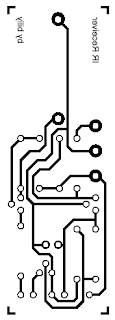
This is the latest version of the Improved Infrared Receiver with Status LED which can control any desktop PC with an ordinary remote control. The project comes along with a small PCB in order to save space. It connects to the serial port as stated in the schematic and uses the freeware Girder (www.girder.nl) software together with Igor’s Plugin (www.cesko.host.sk/girderplugin.htm) to send commands to the PC. The potential uses of this device are countless (control MP3 players, CD and DVD players, radio and TV cards, even move the mouse cursor and shutdown the computer remotely !). Again, note that any ordinary remote control can be used by training Girder to learn its signals !


Project Image


An Improved Infrared Receiver with Status LED


Parts list:
R1 3.3K 1/4W
R2 10K 1/4W
R3 100K 1/4W
R4 10K 1/4W
R5 100K 1/4W
R6 220 1/4W
D1 1N4148
D2 LED 3mm
C1 4.7uF/16V Electrolytic
Q1 BC548
Q2 BC558
IC1 78L05
IC2 TSOP 1736/38/40 (may work with Siemens SFH506xx receivers also)
E1 CR2032 3V battery + PCB base
Misc Three pins to connect the serial cable (optional)

The improvements of this project compared to the ones already published in the internet is that it uses regulated power for the infrared receiver module (TSOP 17xx), has improved sensitivity (worked at a distance of about 10 m), and features a status led which is powered by an external battery source and is driven by two transistors. Upon signal reception, the led blinks to provide a visual feedback to the sender.

Infrared Receiver with Status LED Circuit Daigram


An Improved Infrared Receiver with Status LED


The PCB features narrow tracks (16 mil) so special care should be paid during the construction. The 4.7 uF capacitor is bent towards the board in order to save height if the circuit is to be placed in a small plastic box.


An Improved Infrared Receiver with Status LED

The Girder software for this project was preferred because it is first of all freeware, it is stable and customizable, features a large number of commands and supports user plugins. It is a bit difficult to learn at first, but after a while it deploys a great number of possibilities that other programs (even commercial ones) lack. Nevertheless, with the right corrections (pin changes) this project may be used with other software (WinLIRC, IRAssistant, Miriam, PCRemote) but no such testing has been carried out yet. This is maybe a good point for further search.

ΙR Reciever Pin Numer
Source 7 (RTS)
Ground 5 (GND)
Read 1 (DCD)
Read More..

Thursday, December 19, 2013

Running LED with 4017

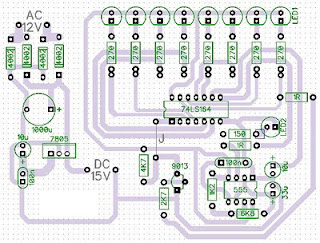
Running LED with 4017 complete with PCB layout. The series of 8 LED current is the basis for creating an 8-point LED. Slightly different from the running LED with IC 4017 (decade counter), 8 running this led is lit in sequence, but that has been previously flame does not die when the led is lit afterwards. 8 led to death after led to the fire-8. Meanwhile in the running LED (decade counter), the system LED lights like "point", there is only one LED that flashes between the tenth led.

Running LED with 4017

The main component is the IC 74LS164 (SHIFT REGISTER), with its timer is astable multivibrator circuit (using IC NE555).

The series will be more efficient when using a stable power supply (regulator) using IC Regulator 7805. Under this scheme a series of stable power supply 5 volts dc.

rangkaian LED berjalan PCB layout

Read More..

Monday, December 16, 2013

Schematic Audio Power Amplifier with IC AN7118S

 *notif : this circuit is stereo power amplifier

Although the schematic power amplifier with IC AN7118S is difficult for lees understood making of  PCB track . But once tried to design on PCB is not so difficult. Because the actual components close together and easy to design it. This Circuit need minimum voltage 1 volt and  maximum voltage 3 volt. It is a low voltage amplifier with power output 2 x 35 m Watt .

Schematic circuit below :


Click to Enlarge

Components Required :

Resistor / Condensator / Capacitor : 4,7Ohm (2x) , 0,01 uF (2x) , 47uf (2x) , 68 pf (2x) , 1uF (2x) ,  22uF (2x) , 220 uF (1x) , 470uf (2x). Condensator / capacitor voltage use 16 volt. Only Condensator on output speaker use voltage 25 volt.

Read More..

Wednesday, December 11, 2013

600 Watt Mosfet Power Amplifier with PCB

Here is a circuit Power Amplifier with output power of more than 600 Watt speakers with impedance of 4 Ohm. Power Amplifier circuit with high power uses n-channel MOSFETs 6 in the output stage alone is giving about 400Watt power. And to make more than 600Watt need to use 12 N-Channel MOSFETs. One of the construction sequence to produce more output power of 900W using 12 IRFP460 MOSFET. Here is a Power Amplifier Circuit Diagram, and the Power Supply is suited for this amplifier. I also include a PCB Layout Models for the power amplifier and its power supply, you can see below.

600 Watt Mosfet Power Amplifier Circuit Diagram
PCB Layout Models 600 Watt Mosfet Power Amplifier

Power Supply for 600 Watt Mosfet Power Amplifier
Power suplly PCB Layout Models 600 Watt Mosfet Power Amplifier
Read More..