Friday, October 24, 2014
Simple Zener Tester Schematic
With the chosen resistors in the circuit the current is approximately: 1mA, 2mA, 5mA, 10mA and 20mA. Great precision is not required.
If meter is chosen here for a small DVM module. However, every other meter is applicable, provided that the input resistance is high enough.
Construction:
The circuit is simple to build on a piece of PCB holes. Note that the DVM module separate from the circuit galvanic isolated power supply needs.
Using
Connect the test zener diode between the terminal A and K. Start with a current of 2mA. This is a safe value for most type zener diodes. Depending on the type of zener diode, may be chosen for a greater current. Than the Zener voltage will vary slightly.
Join the zener diode on backwards, the meter will indicate approximately 0.7V. The same picture shows an ordinary silicon diode. A germanium diode, a voltage of about 0.3 V to 0.4 V indicate when a Schottky approximately 0.2 V indicates.
Connect an LED to A and K, it will be highlighted and the Vforward (LED voltage) of the LED indicate.
The diode / LED failure, the meter displays zero if the voltage at the collector of Q1 is, this is> 25V.

parts List
Bridge rectifier BR1 = 40V 500mA
R1 = 3k3 ¼ W
R2 = 5K6 ¼ W
R3 = 2k7 ¼ W
R4 = 1k ¼ W
R5 = 560 ohm W ½
R6 = 270 ohm ½ W
C1 = 470µF 35V
D1 = 6V2 zener 400mW
Q1 = BC161-16
S1 = on / off switch
S2 = 5 modes 1 mom ignition switch
ENG = The diode under test (Device Under Test)
DVM DVM = module of BACO or Dick Best (input adapted to 200V)

Monday, October 20, 2014
Simple Bells Ring Generator Circuit Schematic
Q2, Q5 and related components act as shape and decay controls of the two tones, trying to imitate as close as possible the bells sound. Their outputs are mixed (R7 & R13), filtered (C5) and boosted by a simple class-A audio amplifier (Q3 & Q4) in order to drive the loudspeaker. The amplifier is switched-on by Q1 when P1 is pressed, then is switched-off some seconds after P1 is released: this time-delay is fixed by C1 & R2. In this way the circuit will draw a negligible current when in stand-by mode.
Circuit diagram:

Parts:
R1,R3,R7,R9,R13_10K 1/4W Resistors
R2_______________1M5 1/4W Resistor
R4______________27K 1/4W Resistor
R5,R11__________47K 1/4W Resistors
R6,R12_________220K 1/4W Resistors
R8_______________2M2 1/4W Resistor
R10_____________33K 1/4W Resistor
C1_______________2µ2 25V Electrolytic Capacitor
C2______________47µF 25V Electrolytic Capacitor
C3,C8___________10µF 25V Electrolytic Capacitors
C4,C7___________10nF 63V Polyester Capacitors
C5,C6__________100nF 63V Polyester Capacitors
C9_______________4µ7 25V Electrolytic Capacitor
C10______________1µF 25V Electrolytic Capacitor
D1-D5_________1N4148 75V 150mA Diodes
IC1__________MC14106 or 40106 Hex Schmitt Inverter IC
Q1_____________BC337 45V 800mA NPN Transistor
Q2,Q3,Q5_______BC238 25V 100mA NPN Transistors
Q4 ____________BC327 45V 800mA PNP Transistor
PH______________Photo resistor (any type) (see Notes)
P1______________SPST Pushbutton (see Notes)
SW1_____________SPST Switch
SPKR____________8 Ohm Loudspeaker
B1______________3V Battery (two 1.5V AA or AAA cells in series etc.)
Parts added to optional modification:
R14____________220K 1/4W Resistor
R15______________1M 1/4W Resistor
Notes:
- To obtain a "Ding-Dong" operation when pushing on P1, no matter when it is released, you must modify the circuit as shown in the frame placed at the low-right corner of the circuit diagram. D4 must be removed. C10 & R15 set the time-delay separating first and second tone.
- To obtain a one-tone-only generator, wire the circuit as in the optional modification, making the following changes:
- C9 = 100nF 63V Polyester Capacitor.
- Omit R9 to R13 & R15; C7, C8 & C10; D2, D4, D5 & Q5.
- Connect to negative supply pins 11 & 13 of IC1 and left open pins 10 & 12.
- An amusing application of this circuit wired as in the original schematic, is to use a photo-resistor in place of P1, then placing the unit near the flashing lamps of your Christmas tree. A soft bell sound may be heard at switch-on and switch-off of the lamp chosen.
- To obtain higher output power you may substitute R8, Q3 & Q4 with an audio amplifier IC like the LM386 or LM380. In this case power supply must be raised to 6 - 12V but at the same time R4 & R10 should be changed to adjust bell-tone frequencies.
- Good tone frequencies are roughly 2000 and 1650Hz respectively.
- When in stand-by mode, current drawing of the circuit is 200µA @ 3V supply: therefore SW1 can be omitted.
Thursday, October 16, 2014
Simple Sleeping Aid Schematic Circuit Diagram
IC2C and IC2D generate two square waves at about 1.2 and 5 Hz respectively. These wave-forms are converted into 60µS pulses at the same frequencies by means of C5 & C6 and mixed at Q1 Base. This transistor drives the Radiator coil with a scalar series of pulses of 60µS length and 9V amplitude. IC1, IC2A & IC2B form the timer section.
C1 & R2 provide auto-reset of IC1 at switch-on. The internal oscillator of IC1 drives the 14 stage ripple counter and, after about 15 minutes, output pin 1 goes high. Pin 3 of IC2A goes low and stops IC2C & IC2D oscillation. If SW2 is left open (Alternate mode operation), after 15 minutes pin 1 of IC1 goes low, pin 3 of IC2A goes high and oscillators are enabled again.
If SW2 is closed (Stop mode operation), the first time output pin 1 of IC1 goes high, the internal oscillator of the IC is disabled by means of D1. Therefore the circuit remains off until a reset pulse is applied to pin 12 by means of P1 or when the whole device is switched-off and then restarted. The same thing occurs when SW1 is switched on 30 or 60 minutes positions, obviously changing time length.
IC2B drives pilot LED D2 which operates in the following three modes:
- flashes quickly and almost randomly when the Radiator coil is driven
- flashes somewhat slowly and regularly when the Radiator coil is pausing during the Alternate mode operation
- is off when the circuit auto-stops (Stop mode operation)
Circuit diagram:

R1 = 1K 1/4W Resistors
R2 = 10K 1/4W Resistor
R3 = 10M 1/4W Resistors
R4 = 2M2 1/4W Resistors
R5 = 1K 1/4W Resistors
R6 = 10M 1/4W Resistors
R7 = 2M2 1/4W Resistors
R8 = 4K7 1/4W Resistors
R9 = 4K7 1/4W Resistors
C1 = 47µF 25V Electrolytic Capacitors
C2 = 100nF 63V Polyester Capacitor
C3 = 330nF 63V Polyester Capacitors
C4 = 330nF 63V Polyester Capacitors
C5 = 15nF 63V Polyester Capacitors
C6 = 15nF 63V Polyester Capacitors
C7 = 47µF 25V Electrolytic Capacitors
D1 = 1N4148 75V 150mA Diodes
D2 = LED (any type) (see Notes)
D3 = 1N4148 75V 150mA Diodes
D4 = 1N4148 75V 150mA Diodes
D5 = 1N4148 75V 150mA Diodes
IC1 = 4060 14 stage ripple counter and oscillator IC
IC2 = 4093 Quad 2 input Schmitt NAND Gate IC
Q1 = BC327 45V 800mA PNP Transistor
L1 = Radiator coil (see Notes)
P1 = SPST Pushbutton
SW1 = 2 poles 4 ways rotary switch
SW2 = SPST Slider Switch
B1 = 9V PP3 Battery, Clip for PP3 Battery
Features:
- Generates a natural electromagnetic-field
- Makes easier to fall asleep
- Induces a prolonged and sound sleep without drugs
- No side effects
Use of this circuit:
- Select a timing option by means of the rotary switch SW1.
- Choose 15, 30 or 60 minutes operation.
- Select "Stop" or "Alternate" mode operation by means of SW2.
- With SW2 closed (Stop mode operation) the electromagnetic radiation stops after the pre-set time is elapsed.
- With SW2 opened (Alternate mode operation) the device operates for the pre-set time, then pauses for the same amount of time: this cycle repeats indefinitely.
- Place the unit under the pillow and sleep like a log.
- To reset a cycle press P1 pushbutton.
Notes:
- L1 is obtained by winding randomly 600 turns of 0.2 mm. enameled wire on a 6 mm. diameter, 40 mm. long, steel bolt. Secure the winding with insulating tape.
- Mean current drawing is about 7mA, decreasing to less than 4mA during pauses when in Alternate mode operation.
- Battery life can be dramatically increased omitting LED D2 and its associated resistor R5.
- Use a plastic box to enclose the circuit: metal cases can severely limit electromagnetic radiation.
Thursday, February 6, 2014
AM Receiver Schematic
AM Receiver Schematic

All general purpose transistors should work in this circuit, I used three BC109C transistors in my prototype.The tuned circuit is designed for medium wave. I used a ferrite rod and tuning capacitor from an old radio which tuned from approximately 550 - 1600kHz. Q1 and Q2 form a compund transistor pair featuring high gain and very high input impedance. This is necessary so as not to unduly load the tank circuit.
The 120k resistor provides regenerative feedback,between Q2 output and the tank circuit input and its value affects the overall performance of the whole circuit. Too much feedback and the circuit will become unstable producing a "howling sound". Insufficient feedback and the receiver becomes "deaf". If the circuit oscillates,then R1s value may be decreased; try 68k. If there is a lack of sensitivity, then try increasing R1 to around 150k. R1 could also be replaced by a fixed resisor say 33k and a preset resistor of 100k. This will give adjustment of sensitivity and selectivity of the receiver.
Transistor Q3 has a dual purpose; it performs demodulation of the RF carrier whilst at the same time, amplifying the audio signal. Audio level varies on the strength of the received station but I had typically 10-40 mV. This will directly drive high impedance headphones or can be fed into a suitable amplifier.
Construction:
All connections should be short, a veroboard or tagstrip layout are suitable. The tuning capacitor has fixed and moving plates. The moving plates should be connected to the "cold" end of the tank circuit, this is the base of Q1, and the fixed plates to the "hot end" of the coil, the juction of R1 and C1. If connections on the capacitor are reversed, then moving your hand near the capacitor will cause unwanted stability and oscillation.
Finally here are some voltagee checks from my breadboard prototype.This should help in determining a working circuit:
All measurements made with a fresh 9volt battery and three BC109C transistors with respect to the battery negative terminal.
Q1 (b) 1.31V
Q2 (b) 0.71V
Q2 (c) 1.34V
Q3 (b) 0.62V
Q3 (c) 3.87V
Wednesday, February 5, 2014
Schematic Audio Power Amplifier with IC AN7105
 |
| Package IC is DIP-18 |
 |
| Click to view Enlarge |
Thursday, January 9, 2014
70W STK amplifier schematic

For this amplifier circuit using three voltage plus, min, and the ground. with a maximum voltage approximately 55Volt DC. And amplifier circuit can use some ic ie IC STK 030, 058, 075, 077, 078, 080, 082, 083, 084, 086. From all the ic I mentioned all of them can be applied to this amplifier circuit. But every ic whether there might be a different maximum voltage or power output, etc.. For this amplifier suitable for use at home, who need a voice soft and tasty. With a maximum output of 70W 8ohm impedance is my take of the highest IC output is STK086.Part List
R1 = 1K
R2 = 56K
R3 = 100R
R4 = 100R
R5 = 56K
R6 = 4.7R
R7 = 2.7K
C1 = 1uF
C2 = 470pF
C3 = 100uF
C4 = 100uF
C5 = 0.047uF
C6 = 47uF
C7 = 1800pF
C8 = 10uF
IC = STK 030, 058, 075, 077, 078, 080, 082, 083, 084, 086.
Monday, December 23, 2013
Schematic Frost Detector Temperature Sensor
Sensor
 We alone charge to ascertain the freezing point with this circuit. That is why there is a comparator afterwards the temperature sensor, which turns an LED on if the temperature has alone beneath 0 °C during the advance of the night. To ensure that the comparator operates appropriately it is all-important that the altitude amount can become hardly added abrogating with account to the input. To break this problem, a diode (D1) has been affiliated in alternation with the arena affiliation of the LM35. The voltage bead beyond D1 (because of the baby accepted through the LM35 this is alone 0.47 V) acts as negative ability supply. Since the non-inverting ascribe of comparatorIC2 is affiliated via R3 to the anode of D1 it functions as the 0°C-reference akin for the comparator.
 Comparator
The comparator is a accepted opamp blazon TLC271, which we configured for basal accepted burning by connecting the bias-select ascribe (pin 8) to the ability accumulation voltage. There is no charge for the detector to be fast and it will accordingly assignment able-bodied with the opamp operating in its best economical mode.
LED D3 provides the frost indication. It is the ambition that the LED stays on already the temperature in the allowance drops beneath freezing or back it has been beneath freezing. To realise this, an agee hysteresis is created with the aid of R3, R4 and D2. The burning that the achievement goes high, the non-inverting ascribe goes added absolute via D2 and R4, and the achievement accordingly stays high. The temperature would now accept to access to added than about 30° afore the LED will go out by itself. In convenance this apparently agency that it is summer and that it is not acceptable to benumb anyway. If charge be, the hysteresis can be added by accretion the amount of R3.
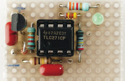
Capacitor C2 is added to accomplish abiding that the LED charcoal off (the ambit is reset) back the ability accumulation is connected. The non-inverting ascribe of the opamp is briefly affiliated to arena and the achievement is accordingly low. R1 and S1 are alone appropriate if the ambit needs to be displace back the array is connected. Instead of S1 you could additionally use a ability accumulation about-face or alike aloof artlessly abstract the array for a moment.
Thrifty Ability supply
Since the ambit is affected to be powered from a array there was a acquainted accomplishment to minimise the ability consumption. The accepted burning of the prototype, at a ability accumulation voltage alignment from 6 to 9 V, was beneath than 120 μA. Back the LED is on, the accepted burning rises to alone 1 mA at 6V and 1.8 mA at 9V, because a low accepted LED is used. In our ancestor we acclimated a green, low-current LED.
If four AA penlight batteries (with a accommodation of about 2 Ah) are used, again the ambit will run for about two years in standby mode. Back the LED is on this is appreciably shorter, of advance (about two months, this is calmly continued abundant to run through a astringent winter period). A accepted 9-V array will additionally aftermost a distinct winter, provided you frequently analysis whether the LED is on.
Finally, a animadversion about the TLC-271CP acclimated here. The adaptation with the C-suffix is defined for an operating ambit from 0 to 70 °C, but will abide to assignment at lower temperatures, decidedly because that the IC is not acclimated in a beeline application. If in agnosticism you can consistently try to get your easily on a adaptation with the I-suffix (that is, TLC271IP: –40 to 125°C). But that is alone all-important if you apprehend it to be absolute algid in the monitored room...
Monday, December 16, 2013
Schematic Audio Power Amplifier with IC AN7118S
 | ||
| Click to Enlarge |
Friday, December 6, 2013
0 15Watt amplifier schematic
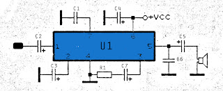
Amplifier circuit is also very suitable when used in fm radio receiver. Supply voltage required 8 - 25 Volt DC with a maximum output power 0.15W.See Schematic below.Part List
R1 = 100R
C1 = 1nF
C2 = 4.7uF
C3 = 10uF
C4 = 100uF
C5 = 47uF
C6 = 4.7nF
U1 = TA7066
Wednesday, November 27, 2013
3 Watt power amplifier schematic
This time I will share a circuit of schematis power amplifier with LM380 IC that has similarities with LM384. Enough with just a few components you have to make this power amplifier circuit . All components with relatively low prices and making a fairly easy. For this amplifier output power has 3W with 4 ohm impedance. Indeed , this amplifier has the output is quite low and certainly will not be maximal if it works on the speakers with high power.

Resistor
R1______________47K
R2______________2.7R 2W
Capacitor
C1______________10uF
C2______________470uF
C3______________100n
C4______________100n
IC
IC1_____________LM380 , LM384
Tuesday, November 26, 2013
Schematic Power Amplifier with IC AN7114 or AN7115
See the Schematic (figure 2.0) and package IC (figure 1.0) :
 |
| Figure 1.0 |
 |
| Figure 2.0 |
Saturday, November 23, 2013
Schematic diagram of a USB player
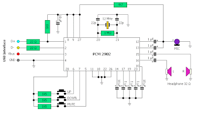 |
| Schematic usb player |
Wednesday, November 20, 2013
Schematic Audio Power Amplifier with IC TDA2822
TDA2822 is manufactered by PHILIPS , its based on this amplifier . Minimum voltage 3 volts and maximum voltage 15 volts. Power output 2 x 1,8 stereo with 4 Ohm impedance. Quiescent current 6 mA , sensitive input is 30 Hz to 18 kHz. See circuit diagram below :

Wednesday, November 13, 2013
50W car audio amplifier schematic circuits
 Car power amplifier uses SI1050GL IC as the main amplifier. The output power 50 Watt 8 ohm mono impedance. Up to 25 Volt DC voltage. with source voltage of this amplifier car battery has to work.
Minimum of 12 Volt battery voltage, less than a sound or audio is issued less than the maximum and less good. You can assemble this circuit amplifier with a schema like this.

C3 = 100uF
U1 = SI1050GL