Showing posts with label amplifier. Show all posts

Friday, October 24, 2014

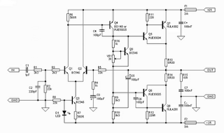
5 Watt Class A Audio Amplifier Circuit diagram

This solid-state push-pull single-ended Class A circuit is capable of providing a sound comparable to those valve amplifiers, delivering more output power (6.9W measured across a 8 Ohm loudspeaker cabinet load), less THD, higher input sensitivity and better linearity. Voltage and current required for this circuit are 24V and 700mA respectively, compared to 250V HT rail and 1A @ 6.3V filament heating for valve-operated amplifiers. The only penalty for the transistor operated circuit is the necessity of using a rather large Heatsink for Q2 and Q3 (compared to the maximum power delivered).In any case, the amount of heat generated by this circuit can be comparable to that of a one-valve amplifier. An optional bass-boost facility can be added, by means of R5 and C5.

 Circuit diagram:

5 Watt Class-A Audio Amplifier Circuit Diagram


Parts:

P1 = 47K
R1 = 100K
R2 = 12K
R3 = 47K
R4 = 8.2K
R5 = 1.5K
R6 = 2.7K
R7 = 100R
R8 = 100R
R9 = 560R-1/2W
R10 = 1R-1/2W
Q1 = BC560
Q2 = BD439
Q3 = BD439
C1 = 10uF-63V
C2 = 10uF-63V
C3 = 47uF-25V
C4 = 100uF-35V
C5 = 150nF-63V
C6 = 220uF-25V
C7 = 220uF-25V
C8 = 1000uF-25V
SPKR = 5W-8R Speaker

Notes:
  • If necessary, R2 can be adjusted to obtain 13V across C8 positive lead and negative ground.
  • Total current drawing of the circuit, best measured by inserting the probes of an Avo-meter across the positive output of the power supply and the positive rail input of the amplifier, must be 700mA. Adjust R8 to obtain this value if necessary.
  • Q2 and Q3 must be mounted on a finned Heatsink of 120x50x25mm. Minimum dimensions.
  • Add R5 and C5 if the bass-boost facility is required.
Read More..

Monday, October 20, 2014

12W Amplifier Circuit Using 741 Op Amp Circuit Diagram

A 12 watt audio amplifier operating on a dual symmetrical supply of ± 12 volts. The 741 provides the required gain while the speaker drive is provided by the complementary Darlingtons T1, T2 and T3, T4.The input signals for the darlingtons are derived from the supply current of the 741. Since R6 is connected to the ground, the positive or negative signal currents also pass through R4 or R5. The voltage drop across these resistors serves as the input signal to the transistor pairs. An overall dc negative feedback from the common collector junction of T2 and T4 stabilises the dc conditions of the circuit and keeps the junction point at zero volts. Hence, no coupling capacitor is required for the speaker.

 12W Amplifier Circuit Using 741 Op Amp Circuit Diagram

12W Amplifier Circuit Using 741 Op Amp Circuit Diagram

PARTS LIST
R1 10KΩ
R2 4.7KΩ
R3 270KΩ
R4 1KΩ
R5 1KΩ
R6 47Ω 1W
C1 50 Pf
C2 0.01 µF
T1 BC178
T2 2N6107
T3 AC108
T4 2N5294
IC LM741
LS1 50W 4Ω
Read More..

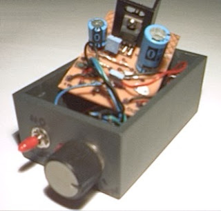
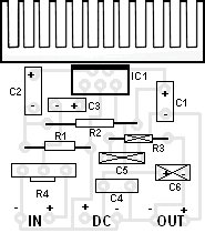
10W Small Audio Amplifier

You can use this powerfull amplifier in any small audio project. It is very small (6.5 x 4.5 cm).It outputs 10W and uses a 9V battery.

10W Small Audio Amplifier


10W Small Audio Amplifier
Component


 10W Small Audio Amplifier
PCB


Componets List
R1 : 6 Ohm
R2 : 220 Ohm
R3 : nothing
R4 : 10 KOhm pontesiometer
C1 : 2200 uF / 25V
C2 : 470 uF / 16V
C3 : 470 nF / 63V
C4 : 100 nF
C5 : nothing
C6 : nothing
IC1 : TDA 2003


Read More..

USB Powered Audio Power Amplifier Circuit Diagram

This USB Powered Audio Power Amplifier Circuit Diagram of multimedia speakers for PCs has single-chip-based design, low-voltage power supply, compatibility with USB power, easy heat-sinking, low cost, high flexibility and wide temperature tolerance. At the heart of the circuit is IC TDA2822M. This IC is, in fact, mono-lithic type in 8-lead mini DIP package. It is intended for use as a dual audio power amplifier in battery-powered sound players. Specs of TDA2822M are low quiescent current, low crossover distortion, supply voltage down to 1.8 volts and minimum output power of around 450 mW/channel with 4-ohm loudspeaker at 5V DC supply input. 

An ideal power amplifier can be simply defined as a circuit that can deliver audio power into external loads without generating significant signal distortion and without consuming excessive quiescent current. This circuit is powered by 5V DC supply available from the USB port of the PC. When power switch S1 is flipped to ‘on’ position, 5V power supply is extended to the circuit and power-indicator red LED1 lights up instantly. Resistor R1 is a current surge limiter and capacitors C1 and C4 act as buffers. Working of the circuit is simple. Audio signals from the PC audio socket/headphone socket are fed to the amplifier circuit through components R2 and C2 (left channel), and R3 and C3 (right channel).

Circuit diagram:
USB Powered Audio Power Amplifier Circuit Diagram

Potmeter VR1 works as the volume controller for left (L) channel and potmeter VR2 works for right (R) channel. Pin 7 of TDA2822M receives the left-channel sound signals and pin 6 receives the right-channel signals through VR1 and VR2, respectively. Ampl i f ied signals for driving the left and right loudspeakers are available at pins 1 and 3 of IC1, respectively. Components R5 and C8, and R6 and C10 form the traditional zobel network. Assemble the circuit on a medium-size, general-purpose PCB and enclose in a suitable cabinet. It is advisable to use a socket for IC TDA2822M. The external connections should be made using suitably screened wires for better result.
Read More..

Friday, September 26, 2014

Simple Automatic Switch For Audio Power Amplifier

Simple Automatic Switch For Audio Power Amplifier.Circuit of an automatic switch for audio power amplifier stage is presented here. The circuit uses stereo preamplifier output to detect the presence of audio to switch the audio power amplifier on only when audio is present. The circuit thus helps curtail power wastage. IC1 is used as an inverting adder. The input signals from left and right channels are combined to form a common signal for IC2, which is used as an open loop comparator. IC3 (NE556) is a dual timer. Its second section, i.e., IC3(b), is configured as monostable multivibrator. Output of IC3(b) is used to switch the power amplifier on or off through a Darlington pair formed by transistors T1 and T2. IC3(a) is used to trigger the monostable multivibrator whenever an input signal is sensed.
Circuit diagram:
Automatic Switch For Audio Power Amplifier-Circuit-Diagram
Automatic Switch For Audio Power Amplifier Circuit Diagram

Under ‘no signal’ condition, pin 3 of IC2 is negative with respect to its pin 2. Hence the output of IC2 is low and as a result output of IC3(a) is high. Since there is no trigger at pin 8 of IC3(b), the output of IC3(b) will be low and the amplifier will be off. When an input singal is applied to IC1, IC2 converts the inverted sum of the input signals into a rectangular waveform by comparing it with a constant voltage which can be controlled by varying potentiometer VR1. When the output of IC2 is high, output pin 5 of IC3 goes low, thus triggering the monostable multivibrator. As soon as the audio input to IC1 stops, pin 5 of IC3 goes high and pin 1 of IC3 discharges through capacitor C3, thus resetting the monostable multivibrator. 

Hence, as long as input signals are applied, the amplifier remains ‘on.’ When the input signals are removed, i.e., when signal level is zero, the amplifier switches off after the mono flip-flop delay period determined by the values of resistor R8 and capacitor C3. If no input signals are sensed within this time, the amplifier turns off—else it remains on. Power supply for the circuit can be obtained from the power supply of the amplifier. Hence, the circuit can be permanently fitted in the amplifier box itself. The main switch of the amplifier should be always kept on. Resistors R1 and R2 are used to divide single voltage supply into two equal parts.

Capacitors C1 and C2 are used as regulators and also as an AC bypass for input signals. Diode D1 is used so that loading fluctuations in power amplifier do not affect circuit regulation. Transisitor T2 acts as a high voltage switch which may be replaced by any other high voltage switching transistor satisfying amplifier current requirements. Value of resistor R10 should be modified for large current requirement. The LED glows when the amplifier is on. The circuit is very useful and relieves one from putting the amplifier on and off every time one plays a cassette or radio etc. 
Read More..

Sunday, February 9, 2014

Stereo High Power Audio Amplifier

Stereo High Power Audio Amplifier

This is a stereo amplifier circuit which has a high output power and excellent sound quality. Amplifier circuit has a very high gain output stage resulting in the deterioration of signal noise distance. This amplifier circuit having an output power of more than 400 Watt x 2 (Stereo) with the speaker impedance 4 Ohm - 8 Ohm. Power supply voltage circuit to supply this high power amplifier with maximum - + 75 Volt DC. Heres the scheme of High Power Amplifier :

High Power Amplifier Circuit Diagram


Read More..

Saturday, February 8, 2014

Car audio amplifier using TDA2003 IC

Car audio amplifier using TDA2003 IC

Easy low power car audio amplifier circuit on TDA 2003. The circuit is Easy to construct. TDA2003 is an integrated radio amplifier from ST Micro electronics that like short circuit protection for all pins, thermal over low harmonic distortion, low cross over distortion etc. In the circuit given here TDA2003 is wired as a mono amplifier operating from a 12V .


Resistors R2 and R3 forms a feedback network that sets the amplifiers gain. C7 input DC de-coupling capacitor and C5 couples the speaker to the amplifiers output. C4 } for improving the ripple rejection C1 and C2 are employed for power filtering. C3 and R1 are used for setting the frequency cut-off. Network comprising of C6 and R4 for frequency stabilization and oscillation.

Notes.

  • Assemble the circuit on a good quality PCB.
  • Heat sinks are necessary for both ICs.
  • The circuit can be operated from 12V DC.
  • S1 is the ON/OFF switch.
Read More..

Friday, February 7, 2014

Stereo TDA2822 audio power amplifier circuit

Stereo TDA2822 audio amplifier circuit
In this series I use IC tda2822M as the main amplifier, but if you want to use in addition to IC TDA2822M you can use ic I mentioned this is KA2209, NJM2073, U2822B, U2823B. Output is issued no more than 4W, which had low output. Supply voltage from 3 volts to 16 volts.


Below its schematics of TDA2822 stereo audio power amplifier

TDA2822 amplifier schematics

Part description
R1 = 4.7R
R2 = 4.7R
C1 = 1uF
C2 = 100uF
C3 = 100uF
C4 = 0.1uF
C5 = 470uF
C6 = 1uF
C7 = 100uF
C8 = 0.1uF
C9 = 470uF
ICs = KA2209 , NJM2073 , TDA2822 , U2822B , U2823B
Read More..

Wednesday, February 5, 2014

Schematic Audio Power Amplifier with IC AN7105

This Schematic Circuit Audio Amplifier use IC AN7105 , minimum voltage 1,5 volt and maximum voltage 9,5 volt. This is a low voltage Amplifier , with output speaker stereo 2 X 0,38 watt . Its so low power amplifier. Impedance speaker is 32 Ohm ,with Frequency 20 Hz -20 kHz.

See this Circuit and package IC AN7105 below :


Package IC is DIP-18

Click to view Enlarge


Read More..

Tuesday, February 4, 2014

3 Volt Operated Power Amplifier Circuits

This is an audio amplifier with the purpose of can live used with a minor 3 volt Battery Operated,Current get through having the status of not much as 5 milliamps.And amplification up to 500 mW.

3 Volt Operated Power Amplifier Circuit Diagram
Which is sufficient to swell the sound from a sound a propos otherwise the disc totter work comatose to the minor speakers obviously. 3 whilst entering the power supply 3-volt circuit IC1 numeral LM386 amplifier IC size is 300-800 mW, Depending on the power supply circuit with,This is from 3-15 volts. just the once entered into the input pin 3,The non inverting pin to amplifier non-return segment.C1 self-control ensue served slice out the blare input to ground.And C2 increases the rate of amplifier,C2 is to add extra denomination.But if the C2 Too much distortion (the C2 be supposed to not exceed 100uF).The output of IC1 is comatose of the pin 5 through C4 coupling audio signals to better and DC frustrate and not voted for to the narrator.on behalf of the audio portion desire in addition be present fed back through R2 and C3 to the extraordinary frequency response better.
Read More..

Thursday, January 30, 2014

170W power amplifier LM4651 and LM4652

170 Watt power amplifier is a power amplifier that is built by IC LM4651 and LM4652.


Part of this power amplifier driver using the LM4651 IC designed specifically for the purpose of the class AB amplifier driver with short circuit protection feature, containing under voltage, thermal shutdown protection and standby functions. Section 170 Watt power amplifier using LM4651 IC with a MOSFET power amplifier is equipped with temperature sensors that will be used by IC LM4651 as controlnya thermal signal. IC IC LM4651 and LM4652 are designed specifically to each other in pairs to create a class AB power amplifier with protection features are detailed. Detailed series of 170 Watt power amplifier can be seen in thethe following figure .

170W power amplifier LM4651 and LM4652

Power amplifier circuit requires supply voltages +22 V DC symmetrical 0-22V. Power Amplifier with IC LM4651 and LM4652 are often used in portable HiFi systems such as powered speakers, power subwoofer and car audio power Booter. D1, D2, D3 and D4 in series 170 watt power amplifier with LM4651 and LM4652 is a 22V zener diode.
Read More..

Monday, January 27, 2014

Simple Amplifier with C945 MJE340 and TIP3055

This simple amplifier does sound good quality Power output about 10 - 14 Watts with Supply voltage about 34 - 36 Volt DC. It requires a preamp in the function of it hasnt got much advance. It requires cumbersome heat up sinks and a great transformer and a enormous power supply and alert wiring, but taking part in the bottom it is enormously regular and it sounds very good. The zener diode rubbish every wave future from the power supply, But you still barely aspire a ripple of 10mV be very successful. The swell triumph the input is enlarged, so the zener diode gets free of with the intention of, but whatever swell in attendance is wish still catch the power stage. The Buffer Stage using transistor C945 , Driver Stage Using MJE340 and Booster Stage using TIP3055 . The Transistor are using NPN transitor.

Simple Amplifier using with MJE340 TIP3055 Circuit
Simple Amplifier using with MJE340 TIP3055 Schematic Circuit Diagram
Read More..

Tuesday, January 21, 2014

OCL Power Amplifier Circuit MJ15003 MJ15004


This Power Amp OCL 100 watt circuit by transistors.They has been an old circuits, but very well amplifier schematic.
We use only all transistor MJ15003 and MJ15004 is the main in circuits, and the power supply +38V 0 -38V 3A. follow stye of OCL amp and They has Spec are
power output : 105watt at 4 ohm load, 88watt at 8 ohms load
input sensitivity : 0.5V
Frequency response : 10-10kHZ +/- 1dB
THD: 0.07% at 50 watt , 0.1% at 100 watt.

This power amp OCL 100w is a very excellent sound quality. Since we provide the circuit in look All direct coupling form is connection join together direct all, to cut-off frequency low-loss problems, the super bass really do not tell who.
The signal Input of the tone controls enter via C1 to the base pin of transistor Q1, which together with the Q2 is differential amplifier, the signal from the collection pin of Q1 supplied to the bas pin of the Q5, which it acts as the pre-driver circuit.
- The transistor Q4 is setting level bias or act as to control Idle current in this circuit. Which we can adjust level idle current by By adjusting the VR1.
- The transistor Q3 acts as a boost trapping.
- The output signal from the Q5 will enter to base pin of Q8,Q9.which acts as the driver circuit. For the signal output to drive the output transistors Q10, Q11.
- Both output transistors Q10, Q11, we used the number on the circuit are MJ15003, MJ15004. This couple can use up to 200W, so not problem in durability.
If you want to save. May be represented by a pair of output are 2N3055, MJ2955 each of the two parallel each other instead.

OCL Power Amplifier Circuit MJ15003,MJ15004
100W OCL Power Amplifier Circuit MJ15003,MJ15004

Creation
-Check the assembly of all equipment to correct the circuit, without the output transistors, Using a voltmeter measure the voltage at the speaker. By also does not have a speaker. At the end of this process was completed and ready to operate immediately.
-Put the power supply to the circuit, then to measure the voltage is 0V or not higher than 0.25V, if not in this means that the circuit failure, need to check first.
-The later, on output transistors, and then use an ammeter to measure the current is supplied with short input circuit. Measuring that positive or negative wire. Then, adjust VR1 until reading about the current 20-40 mA.
- For transistor Q4, when the device successfully. Should be installed on the cooling pad. Which installation of the output transistor. To help control the the bias current output relative to the temperature change of the output transistor.
- The power supply circuit is got by power of transformer T1, which provides voltage to the coil in the secondary coil is 27-0-27 volt, 5 amp.
- The Diodes Bridge rectifier should be not lower than 5 Amp 100V, The filter capacitor C7, C8 we used a 1,000uF 50V, the voltage at the capacitor afer through the filter will can about 38V.
Read More..

Monday, January 20, 2014

700W Power Amplifier with 2SC5200 2SA1943

700W Amplifier Adjust the amplifier power 700W looks calm, but we requirement not put out of your mind to the adjustment happening forcing transistors, the whole relating to-engagement of frequency offset. It is compulsory to change the current insurance rule which serves to guard the final transistors. Their tendency to happen allowable to keep the transistors in the SOAR characteristics. primary it was needed to evaluate all the necessary resistors and subsequently measured to verify the accuracy of the calculations, it is managed with satisfactory results. Peripheral changes required in support of it to be there able to consistently amplifier to supply power. - First you need to restore the 2k2 resistors stylish string with the LEDs on Zenerovými resistors with upper wattage. be enough 1/2W resistors, power loss next to 80V +-based 1W. - therefore was traded 1k2 resistor in the pointer resistor by the side of 620 ohms. 

700W Power Amplifier with 2SC5200, 2SA1943
700W Power Amplifier with 2SC5200, 2SA1943 Circuit Diagram
Which is the initial reap has doubled, so at this point is the overall gain amplifier 40 and the limit excitation is sufficient to 1V rms. - Předbudiči transistors were replaced by stronger MJE15032/33 since KF467/470 are permitted satellite dish current 20mA - by the side of the exciter output stages are used the same transistors for example the output stage. - add up to of terminals of transistors has been increased to eight pairs - It had to occur to compensate designed for the excitation level by calculation a capacitor 10pF to 47pF + 22K appendage. This led to a slight "gradual" amplifiers, but this did not affect the ensuing parameters. This power is tuned correctly in support of this type of terminal transistors 2SA1943/2SC5200. 

With with the purpose of it is a least assessment next to which the amplifier operates stably exclusive of pass by the side of the rising and falling edges of the genuine. - The ultimate adjustment, the adjustment terminal current protection transistor. The SOAR transistor characteristics shows with the intention of the most allowable radio dish current once the voltage of 1.5 A is ideal in favor of cooling, so its essentially not as much of. Therefore, the current protection is customary to 12A, single-arm. This impersonate protection SOAR transistor characteristics. curt-circuit current is regarding 6 A which is about 075A for every transistor. This is far beneath the SOAR characteristics. The mechanical design is relatively clear-cut, the transistors are placed on the two cooling profiles with a height of 66 mm, width 44mm, overall part 260mm. They are twisted contrary to each one other in this way, from the cooling tunnel. Coolers are attaching the nylon aid which allows the compilation of transistors exclusive of washers, and thus better conveying tepla.DPS amplifier next to the top of the tunnel and the transistors are soldered from the underside of PCB.

Read More..

Sunday, January 19, 2014

Hi Fi 25W Power Amplifier Class A

Hi-Fi 25W Power Amplifier (Class-A) Schematics Circuit
Hi-Fi 25W Power Amplifier (Class-A)
Click to view larger
Read More..

Friday, January 17, 2014

150 watts power amplifier circuit

Amplifier circuit is 150 watts power amplifier circuit is quite simple.
This circuit requires only 5 pieces of transistors as the main component of reinforcement. There is no equalizer option on this amplifier circuit because it can be said of this series is very simple, so do not you compare it with that sold in the market which are usually equipped with various sound system and equalizer settings. 


But to add to your collection circuit, this circuit is fairly easy and inexpensive to make and maybe one day you may need as a weak signal booster from your electronic circuit. Or you can also make this amplifier as an amplifier of high frequency signal from the output circuit animal repellent and I guarantee the results are very satisfactory.

150 watts power amplifier circuit


Power supply required is two-polarity power supply is + - 45 volts. Maximum power that can be obtained by this amplifier circuit is around 150 watts. As the volume control you can add potensio or variable resistor 10 Kohm in series at the input. Use dispasi loudspeaker with 150 watts power. Use a heatsink on the transistor-transistor driver loudspeaker or amplifier late as Q1 and Q2.
Read More..

Thursday, January 16, 2014

Spirit Amplifier Schematics

Amplifier circuit built-up is pretty nice not always complex. There are a series of amplifiers that I saw a picture of the kit immediately. The circuit is quite simple, there was the most complex in the pre-amp and its protector.
Click to view larger | CSE-Circuit Schematic Electronics

How a series of ... Op-amp stage 1 is the heart of the circuit, the input stage with enough power to drive the power transistor. Sensor1 ntc & 2 can be attached to the main heatsink, this is optional so it can be eliminated, its functions to lower the bias voltage value if the heatsink overheating. There is no bias trimpot, R6 and R8 instead divide the voltage so we get <= 0.6V at the base driver tr.

If the voltage is just a little more driver transistors can be damaged and could trigger the final transistor is damaged in congregation / pairs. These transistors are used frequently broken, but after replaced by Sanken, safe. Thus the risk of the snaps without a limiter amplifier.

A pair of Q1 & Q2 transisitor drivers are the main transistor amplifier, while the other three pairs of transistors that form the current dumping circuit mode so it will work if there is a signal (especially bass). Final installation of this transistor is in the Blazer, hercules, Eti300w / new Giant. The design of this kind are designed to produce a stomping bass tones, the clarity about the number two, but here the driver transistor is working at grade A. The heat generated quite a bit because of using this mode (current dumping) plus the number of final / power transistor which is more than one pair. I used to use a minimal amount of the final two pairs of transistors to avoid this summer.

Installation of the load resistor should still be there at the foot of the emitter. R16 and C4 are usually intended to stabilize (reduce) the frequency of ultra treble. All use of Sanken transistors. Supply 63V 800VA toroid ct. Reservois capacitors used for stereo 2x 10.000uF/100V Estimated power ... 500W rms at 8 ohms and 1000W at 4 ohms, but supply is limited in the 800VA transformer. Confused with a power output of this? Do not worry about who is more important than that is the loud speaker and the supply has not decreased. With the supply of the transformer between them are quite satisfied to control the speaker says 18 ". If I may be wrong image, R4-220K-C2 in parallel with 68pF
Read More..

Wednesday, January 15, 2014

Very simple stereo amplifier circuit with only need 4 components

This is very very simple circuit audio amplifier  based on IC7057T  , you just use 3 components you can make this circuit . And the minimum voltage is 1 Volts , with just 1 Volt  you can operate this amplifier. Maximum voltage 6,5 volts . Maximum Power output 35mW with 32 ohms impedance. See circuit below :
Very simple stereo amplifier
Read More..

Monday, January 13, 2014

5 8 Watt audio power amplifier

5,8watt amplifier schematics
This amplifier circuit has a power output of a small or too low at 5.8 Watt, which uses IC KA2205. The required voltage for at least 6 volts to 18 volts DC maximum.


Schematics power audio amplifier with IC KA2205

low power amplifier
Component List
C1 = 1uF
C2 = 100uF
C3 = 47uF
C4 = 1000uF
C5 = 0.1uF
C6 = 220uF
IC1 = KA2205

Read More..

Thursday, January 9, 2014

70W STK amplifier schematic

home amplifier schematics
For this amplifier circuit using three voltage plus, min, and the ground. with a maximum voltage approximately 55Volt DC. And amplifier circuit can use some ic ie IC STK 030, 058, 075, 077, 078, 080, 082, 083, 084, 086. From all the ic I mentioned all of them can be applied to this amplifier circuit. But every ic whether there might be a different maximum voltage or power output, etc.. For this amplifier suitable for use at home, who need a voice soft and tasty. With a maximum output of 70W 8ohm impedance is my take of the highest IC output is STK086.
Part List
R1 = 1K
R2 = 56K
R3 = 100R
R4 = 100R
R5 = 56K
R6 = 4.7R
R7 = 2.7K
C1 = 1uF
C2 = 470pF
C3 = 100uF
C4 = 100uF
C5 = 0.047uF
C6 = 47uF
C7 = 1800pF
C8 = 10uF
IC = STK 030, 058, 075, 077, 078, 080, 082, 083, 084, 086.
Read More..