Showing posts with label circuit. Show all posts

Friday, October 24, 2014

Selector Antennas using PIN Diodes Circuit Diagram

This Selector Antennas using PIN Diodes Circuit Diagram selector antennas uses PIN diodes, was designed using common components and is very useful when used various external antennas, this antenna selector uses PIN diodes that eliminate disadvantages of mechanical switches especially at high frequency. 

Capacitors C1 to C4 and C9 are used to prevent the input and output circuit DC. Shock L1 to L5 prevent leakage of HF signal.Shock L1 to L5 can be wound on a ferrite core, using enameled copper wire of 0.3 mm in diameter, two rounds will suffice for entries for VHF and UHF 5 (1 mH is required for VHF and UHF about 5 uH). The circuit was designed for antenna input impedance of 50 or 75 ohms.

Selector Antennas using PIN Diodes Circuit Diagram

Selector Antennas using PIN Diodes Circuit Diagram

Read More..

Selector Antennas using PIN Diodes Circuit Diagram

This Selector Antennas using PIN Diodes Circuit Diagram selector antennas uses PIN diodes, was designed using common components and is very useful when used various external antennas, this antenna selector uses PIN diodes that eliminate disadvantages of mechanical switches especially at high frequency. 

Capacitors C1 to C4 and C9 are used to prevent the input and output circuit DC. Shock L1 to L5 prevent leakage of HF signal.Shock L1 to L5 can be wound on a ferrite core, using enameled copper wire of 0.3 mm in diameter, two rounds will suffice for entries for VHF and UHF 5 (1 mH is required for VHF and UHF about 5 uH). The circuit was designed for antenna input impedance of 50 or 75 ohms.

Selector Antennas using PIN Diodes Circuit Diagram

Selector Antennas using PIN Diodes Circuit Diagram

Read More..

Low drop Regulator with Indicator Circuit Diagram

Even today much logic is still powered from 5 volts and it then seems obvious to power the circuit using a standard regulator from a rectangular 9-V battery. A disadvantage of this approach is that the capacity of a 9-V battery is rather low and the price is rather high. Even the NiMH revolution, which has resulted in considerably higher capacities of (pen-light) batteries, seems to have escaped the 9-V battery generation. It would be cheaper if 5 volts could be derived from 6 volts, for example. That would be 4 ‘normal’ cells or 5 NiMH- cells. Also the ‘old fashioned’ sealed lead- acid battery would be appropriate, or two lithium cells.
 
Circuit diagram : 
Low-drop Regulator with Indicator-Circuit-Diagram
Low-drop Regulator with Indicator Circuit Diagram
 
Using an LP2951, such a power supply is easily realised. The LP2951 is an ever- green from National Semiconductor, which you will have encountered in numerous  Elektor Electronics designs already. This IC can deliver a maximum current of 100 mA at an input voltage of greater than 5.4 V. In addition to this particular version, there are also versions available for 3.3 and 3 V output, as well as an adjustable version.  In this design we have added a battery indicator, which also protects the battery from too deep a discharge. As soon as the IC has a problem with too low an input voltage, the ERROR output will go low and the regulator is turned off via IC2d, until a manual restart is provided with the RESET pushbutton.
 
The battery voltage is divided with a few resistors and compared with the reference voltage (1.23 V) of the regulator IC. To adapt the indicator for different voltages you only need to change the 100-k resistor. The comparator is an LP339. This is an energy-friendly version of the LM339. The LP339 consumes only 60 µA and can sink 30 mA at its output. You can also use the LM339, if you happen to have one around, but the current consumption in that case is 14 times higher (which, for that matter, is still less than 1 mA).
 
Finally, the LP2951 in the idle state, consumes about 100 µA and depend- ing on the output current to be deliv- ered, a little more. 


Read More..

TV Video Transmitter Circuit Diagram

This circuit is a video transmitter that has many uses, such as video cameras, security cameras, satellite receivers, DVD, Video Games, etc. .. The circuit transmits 470-580MHz and can be tuned in the UHF channels 21-34. The video transmitter can reach up to 300 meters in open field using a wire antenna of 10-20 cm.
TV Video Transmitter Circuit Diagram

TV Video Transmitter Circuit Diagram


Video Transmitter

Transmitter can work with a voltage from 9 to 15 volts. However, you can also use a 9v battery. Oscillator is based around BF199 and BFR90 is the RF transistors. If necessary, the transmission power can be increased by replacing with BFR90 transistor 2N3886.
Read More..

5 Watt Class A Audio Amplifier Circuit diagram

This solid-state push-pull single-ended Class A circuit is capable of providing a sound comparable to those valve amplifiers, delivering more output power (6.9W measured across a 8 Ohm loudspeaker cabinet load), less THD, higher input sensitivity and better linearity. Voltage and current required for this circuit are 24V and 700mA respectively, compared to 250V HT rail and 1A @ 6.3V filament heating for valve-operated amplifiers. The only penalty for the transistor operated circuit is the necessity of using a rather large Heatsink for Q2 and Q3 (compared to the maximum power delivered).In any case, the amount of heat generated by this circuit can be comparable to that of a one-valve amplifier. An optional bass-boost facility can be added, by means of R5 and C5.

 Circuit diagram:

5 Watt Class-A Audio Amplifier Circuit Diagram


Parts:

P1 = 47K
R1 = 100K
R2 = 12K
R3 = 47K
R4 = 8.2K
R5 = 1.5K
R6 = 2.7K
R7 = 100R
R8 = 100R
R9 = 560R-1/2W
R10 = 1R-1/2W
Q1 = BC560
Q2 = BD439
Q3 = BD439
C1 = 10uF-63V
C2 = 10uF-63V
C3 = 47uF-25V
C4 = 100uF-35V
C5 = 150nF-63V
C6 = 220uF-25V
C7 = 220uF-25V
C8 = 1000uF-25V
SPKR = 5W-8R Speaker

Notes:
  • If necessary, R2 can be adjusted to obtain 13V across C8 positive lead and negative ground.
  • Total current drawing of the circuit, best measured by inserting the probes of an Avo-meter across the positive output of the power supply and the positive rail input of the amplifier, must be 700mA. Adjust R8 to obtain this value if necessary.
  • Q2 and Q3 must be mounted on a finned Heatsink of 120x50x25mm. Minimum dimensions.
  • Add R5 and C5 if the bass-boost facility is required.
Read More..

Simple Proportional Temperature Controller Circuit Diagram

This temperature controller operates as a pulse snatching device, which allows it to run at its own speed and tum on at the zero crossing of the line frequency. Zero crossing tum-on reduces the generation of line noise transients. TMOS Power FET, Ql, is used to tum on a heater. Temperature sensor D6 provides a de voltage proportional to temperature that is applied to voltage-tofrequency converter Ul. Output from Ul is a pulse train proportional to temperature offset that is applied to the input of triac optoisolator U2. 


The anode supply for the triac is a 28 V pk-pk, full-wave rectified sine wave. The optoisolator ORs the pulse train from Ul with the zeroTrossing of U2`s anode supply, supplying a gate tum on signal for Ql. Therefore, TMOS power FET Ql can only tum the heater on at the zero crossing of the applied sine wave. The maximum temperature, limited by the sensor and the insulation of the wire, is 130°C for the components shown. 
Read More..

Test Multiteste LEDs Polarity Continuity Resistance Circuit

What do you think of building a simple LED tester, so you can test the integrity of the components before soldering directly to the PCB. It reduces the task of testing the meter components using the circuit with LED gives an indication about the good or bad condition of the component.

Test Multiteste LEDs - Polarity - Continuity - Resistance Circuit

Test Multiteste LEDs - Polarity - Continuity - Resistance Circuit


When a component is placed in the circuit and establishes electrical continuity T1 receives base current through R1. When T1 conducts, the green LED turns on and off the red LED. This indicates that the component to be tested is good. If the component is bad, will not have electrical continuity and T1 remains off. In this state only the red LED light indicating that the component is bad.
 
  Polarity

Connect the red end of the positive range to the circuit board and to test the black edge point. Circuit board under test to be lit
Green LED ON - positive feed. Green LED off and red LED - or no negative supply voltage.
 
Continuity

Connect both ends red and black throughout the test points
Green LED-Continuity. LED red if there is no continuity
Resistor. 1 ohm to 500K

Alloy ends red and black on each side of resistor
Green LED Resistor-OK. Green LED off and red LED Resistor burned
 
Electrolytic capacitor

Red probe tip to positive and black for negative capacitor.
Green LED turns on and off gradually and then red lights, Capacitor good. Red LED lights up steadily bad capacitor

LED diodes, photodiodes, infrared diodes


The Red pontaa probe anode and cathode Black
Green LED - LED Good and Green LED off and red LED diode, or LED bad
Change the direction of the tips. If the green LED diode or LED is open


LDR

Tips in red and black leads of the LDR
Under the light, green LED and red LED fading. covering the LDR with your hand. Green LED off LDR good
Read More..

Simple 555 Tester Circuit Diagram


Simple 555 Tester Circuit Diagram

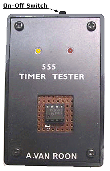
This is a Simple 555 Tester Circuit Diagram. The IC 555 is a widely used timers, control circuits, PWM, alarms, etc.. Often we set up a circuit that does not work or works differently than expected, this time the ideal is a test circuit for this IC. 

This test circuit 555 is connected as an astable multivibrator when the button switch S1 is pressed, the LEDs D1 and D2 flash alternately. Ie, when the output is high D2 will light when the output is low D3 will light, and the other a Hi Lo. The speed of flashes is determined by the components R1, R2 and C1.Pressing the S1 test the 555 starts and any change in the IC flashes may consider to be defective.

Simple 555 Tester Circuit Diagram

Read More..

Thursday, October 23, 2014

High Power LEDs up to 15 Amperes Circuit Diagram

This High Power LEDs up to 15 Amperes Circuit Diagram employs a simple scheme that limits the current flow to the LED, you can easily modify the circuit, and can change the power just replacing the value of R2. You can use a DC source of any tensions between 9V to 15V.Para powers or other LEDs just use the approximate formula:

Current (I) = 0.8/R2 where I is the current specified by the LED manufacturer. Value of I this conductor is 10A. Use R2 = 0.8/Current formula (I) to determine R2.

High Power LEDs up to 15 Amperes Circuit Diagram

High Power LEDs up to 15 Amperes Circuit Diagram


Parts List

Q1 2N3055 or similar NPN transistor
R1 1W 220ohms
D1, D2 1N4001 silicon diode or rectifier

See R2 power for each LED

R2 for 1W LED 1W 2.7ohms
R2 LED to 1.5 ohms 1W 3W
5W LED R2 to 0.6 ohms or 2 x parallel 1.2-ohms/1W
Read More..

Simple Alkaline Cell Charger Circuit Diagram

This is the Simple Alkaline Cell Charger Circuit Diagram. This charger works as two channel current limited voltage source 1.6 V. Low charge current allows charging deep discharged cells (0.7 - 0.8 V) and non-rechargeable cells. Charge current can be changed by R9 and R10. With 470 Ohm is approx 7 mA. LED1 and LED indicates when cell voltage reached 1.6 V and cell is fully charged. 

If power supply is disconnected, reverse discharging current is negligibly (less than 1 microA). For this feature is operational amplifier type LM324 recommended or similar type with p-n-p transistor on input. Non-rechargeable cells can be charged, but their capacity will be significantly less than rechargeable cells

Alkaline Cell Charger Circuit Diagram


Parts list

R1 2,2 kohm
R2 10 kohm
R3 2,7 kohm
R4 15 kohm
R5, R6 5,6 kohm
R7, R8 22 kohm (viz text) /
depend on R9, R10 (approx. 50 times greater than R9, R10)
R9, R10 470 ohm (see text) / change charge current
R11, R12 1 kohm (See text) / change LEDs current
R13 1 kohm, SMD1206
C1 100 nF, ceramic
D1, D2 1N4148 etc.
T1, T2 2SC945 etc.
IC1 TL431C
IC2 LM324
LED1 until LED3 Any LED 3 mm with low power consumption /
any low power 3 mm LEDs
  Housing Articles/ cell cases AA, AAA
  pcb bcs67 / PCB board see fig. 2
Read More..

Monday, October 20, 2014

Car Charger And Switcher Circuit For SLA Battery

This circuit was devised to switch power to a Peltier cooler in a vehicle. Power to the load from the vehicle’s battery is switched by a SPDT relay while the ignition switch is turned on and from the SLA auxiliary battery when the ignition is off.

The SLA battery is charged from the vehicle’s battery. When the engine is running, the voltage remains fairly constant, which greatly simplifies the charging circuit. If the SLA battery is fully charged, any further charging current from the vehicle battery is limited by a 3.3W 5W resistor (R1). If the SLA battery is deeply discharged, the voltage drop across this resistor will be enough to bias on PNP transistor Q1. This will turn on P-channel Mosfet Q2 and it will provide further charging current via R2, effectively becoming a 2-step charger.

Since the paralleled resistors (R1 & R2) have a lower combined voltage drop, Q1 will receive lower base bias, which in turn will cause Mosfet Q2 to fully saturate. This positive feedback creates a clean transition between the two states and prevents Q2 from over-dissipating by being partially on. The current then will ramp down until the battery is only receiving a trickle charge and the voltage drop across the paralleled resistors is only a few dozen millivolts. Schottky diode D1 prevents the SLA battery from discharging into the vehicle’s accessory circuits when the engine is off.

Two safety devices are included in the circuit, the first being in-line fuse F1 which will prevent serious damage in case of shorts. In addition, a PTC resettable thermistor (RT1) protects the battery from sustained over-currents during the charging phase. It is a 1.85A hold, 3.70A trip device at 23°C. Since it has a positive temperature coefficient, at 70°C, these ratings decrease to 1A and 2A for hold and trip respectively, which can further protect the battery.

Circuits Diagram

Lastly, to protect the SLA battery from deep discharge, a low voltage disconnect is included. This is centred around REG1, a voltage reference configured as a comparator. Its reference (REF) input is connected to a voltage divider, as long as "enable" switch S1 is closed.

Whenever the voltage at REG1’s reference terminal exceeds 2.5V, its anode will be pulled low, biasing on PNP transistor Q3. Q3 provides positive feedback via the 270kΩ resistor and diode D2 to turn on N-channel Mosfet Q4, which allows the load to be powered up.

If the SLA battery voltage drops below 10V, the reference terminal will fall below 2.5V and the anode of REG1 will go high, thereby removing bias from Q3 and turning off Q4 to disconnect the load and prevent deep discharge. LED1 indicates when power is being applied to the load.
Read More..

Build a FM Booster Circuit Diagram

A low-cost circuit of an FM booster that can be used to listen programs from distant FM stations clearly. The circuit comprises a common-emitter tuned RF preamplifier wired around VHF/UHF transistor 2SC2570 ( C2570). this FM booster circuit is constructed using few common components( not require some special components ) and provide a very good gain .to calibrate this circuit you need to adjust input/output trimmers (VC1/VC2) for maximum gain.

 FM Booster C/ ircuit Diagram

 Input coil L1 consists of four turns of 20SWG enamelled copper wire (slightly space wound) over 5mm diameter former. It is tapped at the first turn from ground lead side. Coil L2 is similar to L1, but has only three turns. Both of the trimmers are 22pF value. This FM radio signal booster needs to be powered by a 12 volts DC power supply .
Read More..

Latest TDA2030 Complete Tone Control Circuit Diagram

This is the Simple IC TDA2030 Complete tone Control Circuit Diagram. This circuit that use IC TDA2030, but this series is equipped with a tone control. Tone controls include Bass, Treble, and Volume. Power amplifier and tone control has been put together in a single PCB. This amplifier is a mono amplifier type, can be modify for guitar amplifiers. 

If not coupled amplifier (mic preamp) then you must deactivated potensio treble and bass, why? because if not using a mic preamp and still maintain potensio treble and bass sound input (input) from the guitar will not or the maximum discharge is not tight on the speakers. So you must deactivated a way to decide which directly connected capacitor with the tone control circuit, and capacitor were connected directly to potensio volume and input jack.

 TDA2030 Complete Tone Control Circuit Diagram

Latest TDA2030 Complete Tone Control Circuit Diagram


PCB Layout

 TDA2030 Complete Tone Control Circuit Diagram PCB

 TDA2030 Complete Tone Control Circuit Diagram PCB

 TDA2030 Complete Tone Control Circuit Diagram PCB

Read More..

Simple Function Generator Circuit Diagram using NE566

Simple circuit function generator that generates square wave and triangular or sawtooth. The frequency is determined by R and C1. For the sawtooth wave output is on pin 4 and the voltage of 6 V, while for the square wave output is on pin 3. The function generator circuit uses only one 566 and can be connected to output amplified audio. The frequency is set by potentiometer R2.


 Function generator circuit using NE566 Circuit Diagram

 Function generator circuit using NE566 Circuit Diagram

Read More..

Ceiling Fan Regulator Motor Speed Control Circuit Diagram

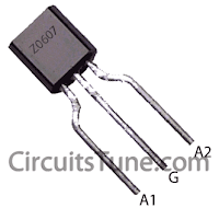
This is a simple ceiling fan regulator circuit diagram. It is used to control the speed of a ceiling fan. In the other words it is an AC motor speed controller circuit, as because its control the speed of a AC motor(Ceiling Fan).  This ceiling fan regulator circuit built with few numbers of parts. The circuit mainly  based on Z0607 TRIAC. This is a low power AC semiconductor device. Generally which is used to controlling speed of low power ac motor speed. 

Circuit Diagram of Ceiling Fan Regulator :

Ceiling fan regulator-motor speed control circuit wiring diagram
Fig: Ceiling fan regulator circuit- AC motor speed controller 
In this ceiling fan regulator circuit, R1=500KΩ is a variable resistor that is used to adjust the fan speed. Capacitor C1 2A104J is a Polyester film capacitor.

Pin Diagram of  TRIAC(T1)- Z0607: 


Z0607 TRIAC Pin Diagram
Fig: Z0607-TRIAC Pin diagram

Pin Diagram of Variable Resistor R1:


Pin Diagram of Variable Resistor
Fig: Pin Diagram of Variable Resistor

Parts List Ceiling Fan Motor Speed Controller circuit:

T1 = Z0607 -TRIAC
D1 = DB3 C312 -DIAC
R1 = 500KΩ -Variable Resistor
R2 = 37KΩ -Resistor
C1 = 2A104J -Polyester film capacitor.
M1 = Single Phase AC Motor (Ceiling Fan)-220V,50Hz


Source
Read More..

12W Amplifier Circuit Using 741 Op Amp Circuit Diagram

A 12 watt audio amplifier operating on a dual symmetrical supply of ± 12 volts. The 741 provides the required gain while the speaker drive is provided by the complementary Darlingtons T1, T2 and T3, T4.The input signals for the darlingtons are derived from the supply current of the 741. Since R6 is connected to the ground, the positive or negative signal currents also pass through R4 or R5. The voltage drop across these resistors serves as the input signal to the transistor pairs. An overall dc negative feedback from the common collector junction of T2 and T4 stabilises the dc conditions of the circuit and keeps the junction point at zero volts. Hence, no coupling capacitor is required for the speaker.

 12W Amplifier Circuit Using 741 Op Amp Circuit Diagram

12W Amplifier Circuit Using 741 Op Amp Circuit Diagram

PARTS LIST
R1 10KΩ
R2 4.7KΩ
R3 270KΩ
R4 1KΩ
R5 1KΩ
R6 47Ω 1W
C1 50 Pf
C2 0.01 µF
T1 BC178
T2 2N6107
T3 AC108
T4 2N5294
IC LM741
LS1 50W 4Ω
Read More..

How Put that Light Out! Circuit Diagram

If you forget to switch off the light after leaving a seldom used room (such as the loft), there’s a strong likelihood that it could remain lit for months, running up an expensive power bill in the process. How can we prevent this waste?

It’s not hard for electronics enthusiasts to design a little circuit to mitigate the effects of absentmindedness. The notion is simple; if the light is left on when the hatch or door is closed, a rhythmic sounder/buzzer signal produces an alarm that hopefully will not be masked by other noise.

Circuit Diagram:

How Put that Light Out! Circuit Diagram

The circuit is powered as long as the lamp bulb is switched on by light switch S1. If the reed switch S2 then signals that the hatch has been closed, the sounder operates. The red LED, mounted outside the loft next to the entry hatch, also indicates that the lamp up there needs to be switched off. The circuit does not use a transformer, meaning that the whole circuit is at mains potential. For this reason the components must be placed inside an insulated plastic case for protection, with no way that people can touch any part of the circuit (this includes the sounder).

The connecting wires to the LED and the reed switch contact must be fully protected to the same touch-proof degree too. For the sounder you can use any type that operates on direct current in the region between 1 V and 3 V. In this circuit the operating voltage is limited by the LED connected in parallel to the buzzer. Using a red LED will provide around 1.7 V to the sounder. The current requirement of this kind of miniature sounder is about 5 mA.

Author: Stefan Hoffmann - Copyright: Elektor
Read More..

Simple Timer with Transistor Circuit Diagram

The below Simple Timer with Transistor Circuit Diagram is a simple timer that uses only two Darlington transistors and a capacitor base to generate a delay. When SW1 is pressed, the timer starts, the time setting is set by VR1. The duration of the timer is given by the values ​​of the potentiometer VR1 and the capacitor C1 that this circuit is 220 pF. To reach other durations of time must change the values ​​of these two components.

Timer with Transistor Circuit Diagram

Simple Timer with Transistor Circuit Diagram

Read More..

USB Powered Audio Power Amplifier Circuit Diagram

This USB Powered Audio Power Amplifier Circuit Diagram of multimedia speakers for PCs has single-chip-based design, low-voltage power supply, compatibility with USB power, easy heat-sinking, low cost, high flexibility and wide temperature tolerance. At the heart of the circuit is IC TDA2822M. This IC is, in fact, mono-lithic type in 8-lead mini DIP package. It is intended for use as a dual audio power amplifier in battery-powered sound players. Specs of TDA2822M are low quiescent current, low crossover distortion, supply voltage down to 1.8 volts and minimum output power of around 450 mW/channel with 4-ohm loudspeaker at 5V DC supply input. 

An ideal power amplifier can be simply defined as a circuit that can deliver audio power into external loads without generating significant signal distortion and without consuming excessive quiescent current. This circuit is powered by 5V DC supply available from the USB port of the PC. When power switch S1 is flipped to ‘on’ position, 5V power supply is extended to the circuit and power-indicator red LED1 lights up instantly. Resistor R1 is a current surge limiter and capacitors C1 and C4 act as buffers. Working of the circuit is simple. Audio signals from the PC audio socket/headphone socket are fed to the amplifier circuit through components R2 and C2 (left channel), and R3 and C3 (right channel).

Circuit diagram:
USB Powered Audio Power Amplifier Circuit Diagram

Potmeter VR1 works as the volume controller for left (L) channel and potmeter VR2 works for right (R) channel. Pin 7 of TDA2822M receives the left-channel sound signals and pin 6 receives the right-channel signals through VR1 and VR2, respectively. Ampl i f ied signals for driving the left and right loudspeakers are available at pins 1 and 3 of IC1, respectively. Components R5 and C8, and R6 and C10 form the traditional zobel network. Assemble the circuit on a medium-size, general-purpose PCB and enclose in a suitable cabinet. It is advisable to use a socket for IC TDA2822M. The external connections should be made using suitably screened wires for better result.
Read More..

Simple Bells Ring Generator Circuit Schematic

This circuit generates a dual-tone bells ringing similar to most door-bell units. It can be used in many applications other than door-bell. In the Notes below several options will be given in order to suit different needs. The circuit as shown in the diagram generates a "Ding-tone" when P1 is pressed and a "Dong-tone" when P1 is released. IC1D is the first-tone frequency generator and IC1F generates the second-tone.

Q2, Q5 and related components act as shape and decay controls of the two tones, trying to imitate as close as possible the bells sound. Their outputs are mixed (R7 & R13), filtered (C5) and boosted by a simple class-A audio amplifier (Q3 & Q4) in order to drive the loudspeaker. The amplifier is switched-on by Q1 when P1 is pressed, then is switched-off some seconds after P1 is released: this time-delay is fixed by C1 & R2. In this way the circuit will draw a negligible current when in stand-by mode.

Circuit diagram:
 bells ring generator schematic circuit diagram
Bells Ring Generator Schematic Circuit Diagram

Parts:

R1,R3,R7,R9,R13_10K 1/4W Resistors
R2_______________1M5 1/4W Resistor
R4______________27K 1/4W Resistor
R5,R11__________47K 1/4W Resistors
R6,R12_________220K 1/4W Resistors
R8_______________2M2 1/4W Resistor
R10_____________33K 1/4W Resistor
C1_______________2µ2 25V Electrolytic Capacitor
C2______________47µF 25V Electrolytic Capacitor
C3,C8___________10µF 25V Electrolytic Capacitors
C4,C7___________10nF 63V Polyester Capacitors
C5,C6__________100nF 63V Polyester Capacitors
C9_______________4µ7 25V Electrolytic Capacitor
C10______________1µF 25V Electrolytic Capacitor
D1-D5_________1N4148 75V 150mA Diodes
IC1__________MC14106 or 40106 Hex Schmitt Inverter IC
Q1_____________BC337 45V 800mA NPN Transistor
Q2,Q3,Q5_______BC238 25V 100mA NPN Transistors
Q4 ____________BC327 45V 800mA PNP Transistor
PH______________Photo resistor (any type) (see Notes)
P1______________SPST Pushbutton (see Notes)
SW1_____________SPST Switch
SPKR____________8 Ohm Loudspeaker
B1______________3V Battery (two 1.5V AA or AAA cells in series etc.)
Parts added to optional modification:
R14____________220K 1/4W Resistor
R15______________1M 1/4W Resistor

Notes:
  • To obtain a "Ding-Dong" operation when pushing on P1, no matter when it is released, you must modify the circuit as shown in the frame placed at the low-right corner of the circuit diagram. D4 must be removed. C10 & R15 set the time-delay separating first and second tone.
  • To obtain a one-tone-only generator, wire the circuit as in the optional modification, making the following changes:
  • C9 = 100nF 63V Polyester Capacitor.
  • Omit R9 to R13 & R15; C7, C8 & C10; D2, D4, D5 & Q5.
  • Connect to negative supply pins 11 & 13 of IC1 and left open pins 10 & 12.
  • An amusing application of this circuit wired as in the original schematic, is to use a photo-resistor in place of P1, then placing the unit near the flashing lamps of your Christmas tree. A soft bell sound may be heard at switch-on and switch-off of the lamp chosen.
  • To obtain higher output power you may substitute R8, Q3 & Q4 with an audio amplifier IC like the LM386 or LM380. In this case power supply must be raised to 6 - 12V but at the same time R4 & R10 should be changed to adjust bell-tone frequencies.
  • Good tone frequencies are roughly 2000 and 1650Hz respectively.
  • When in stand-by mode, current drawing of the circuit is 200µA @ 3V supply: therefore SW1 can be omitted.
Source: Red Free Circuit Models
Read More..